Portable Radio Reference Design — Assembly Instructions
These are the assembly instructions for the radio.
Stage 1 — Partial Assembly
Belly Plate
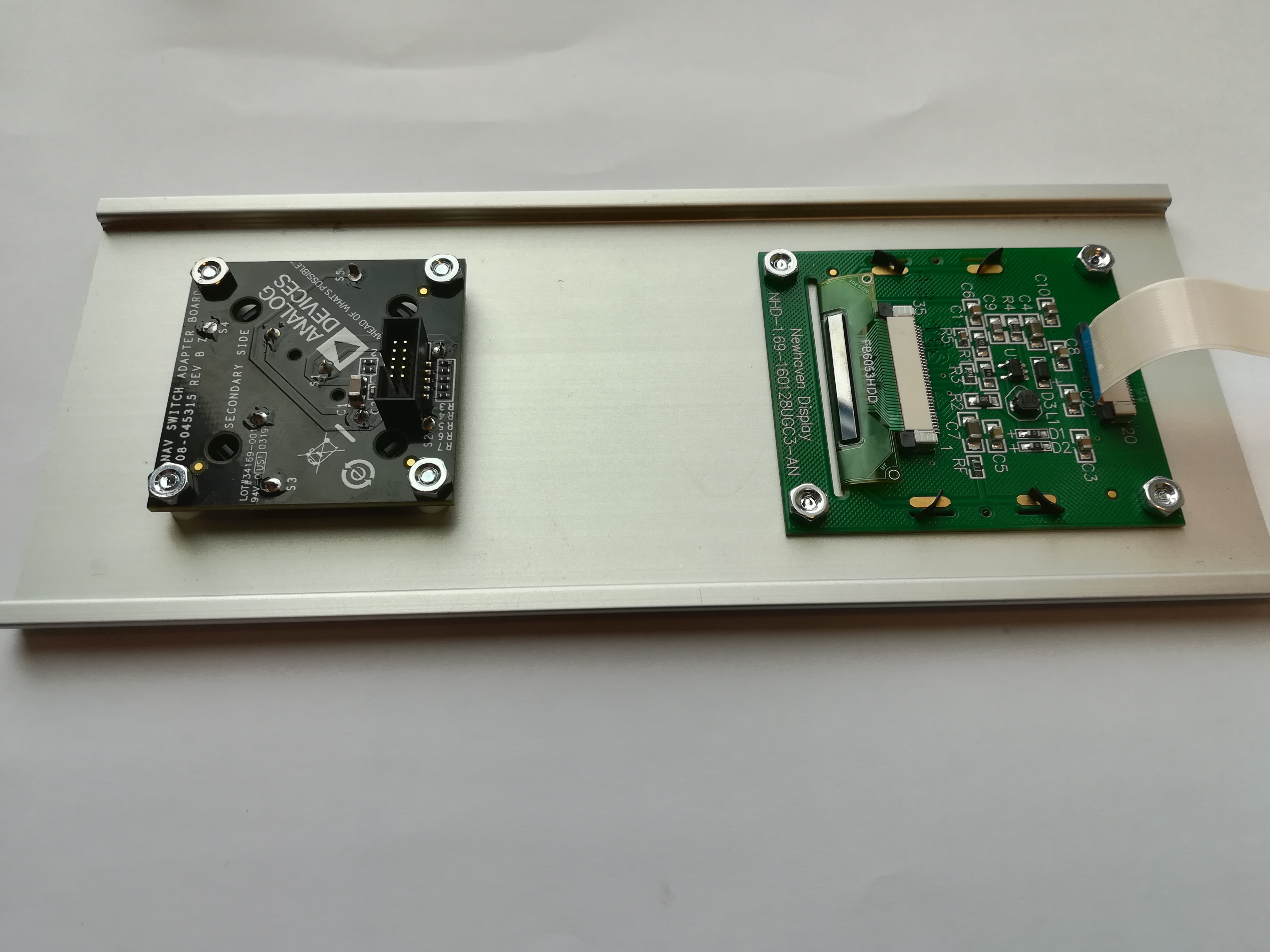
OLED Installation
Cut a strip of electric tape to place over the exposed vias found on the OLED PCB.
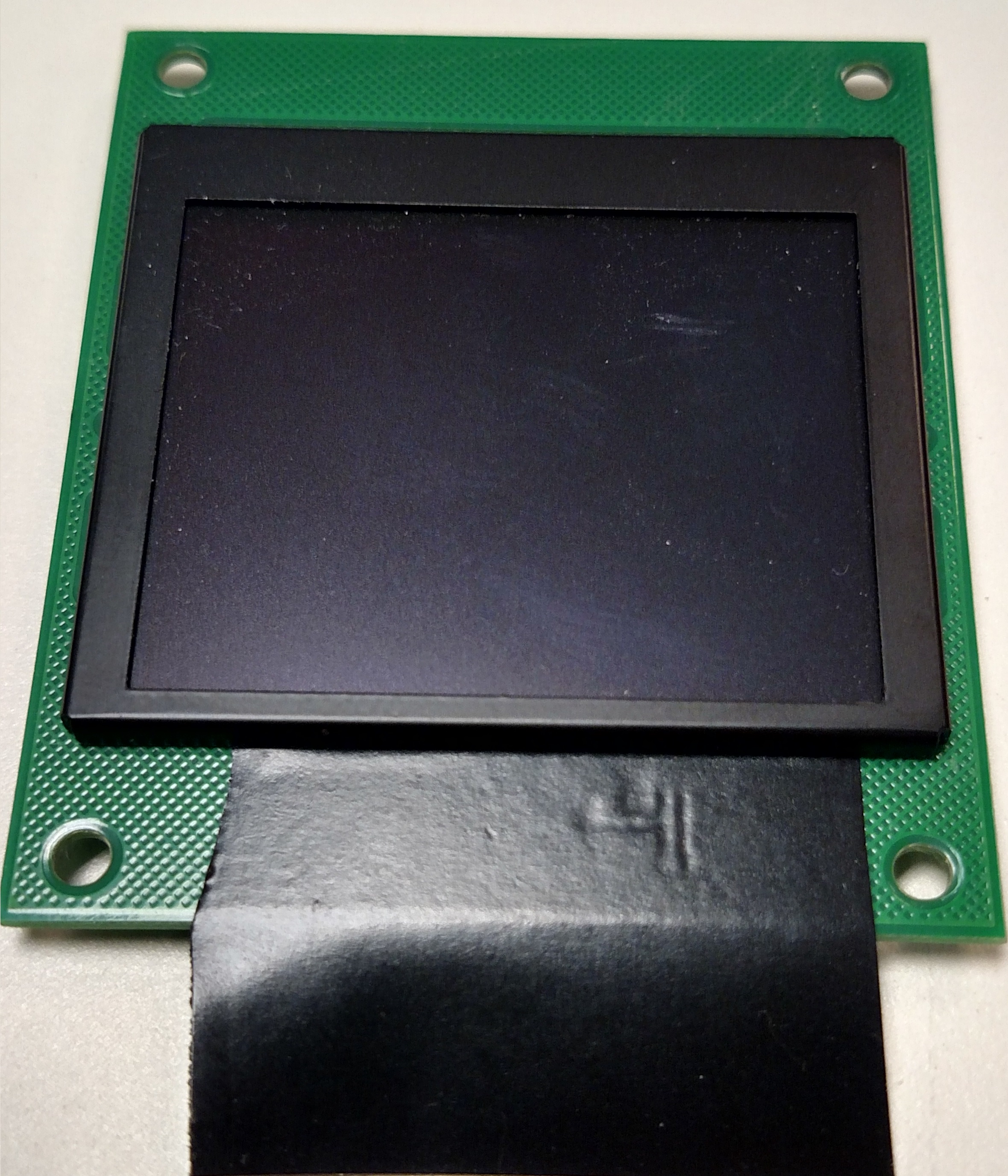
Place the OLED into the rectangular opening.
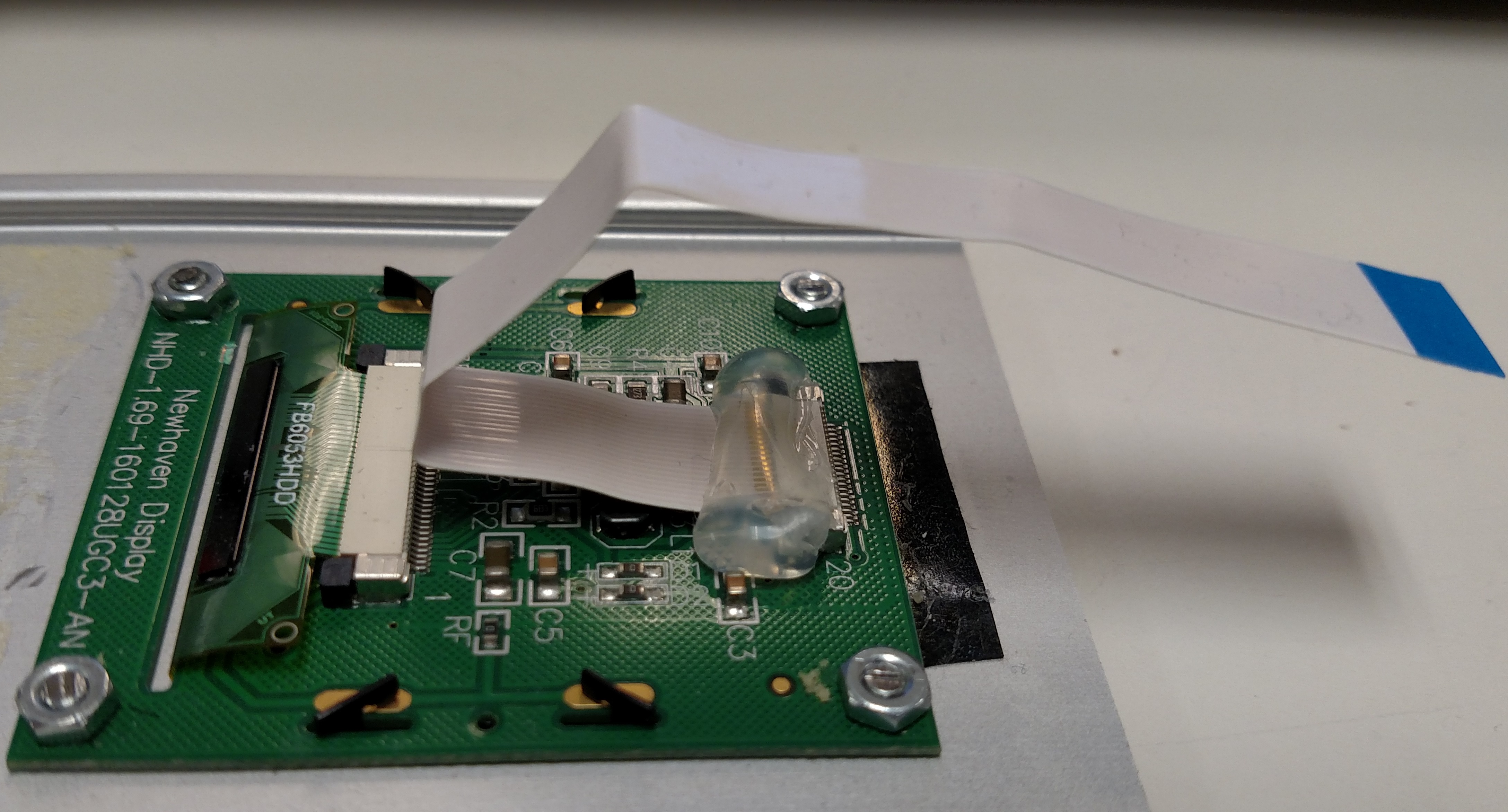
Place 4× M2.5 × 4mm screws through the belly plate and OLED. Apply Loctite. Attach 4× M2.5 nuts and tighten. Cut off the ends of the screw if it extends beyond the nut.
Insert a 20-position FMC cable into the OLED connector with the exposed copper facing away from the PCB. Close the black bracket to secure the cable.
Apply hot glue to the connector and part of the cable so it cannot be accidentally removed.
Warning
Be careful removing this glue — too much force can damage the OLED connector.
Bend the cable backwards so it sticks out past the end of the belly plate.
Nav Switch Installation
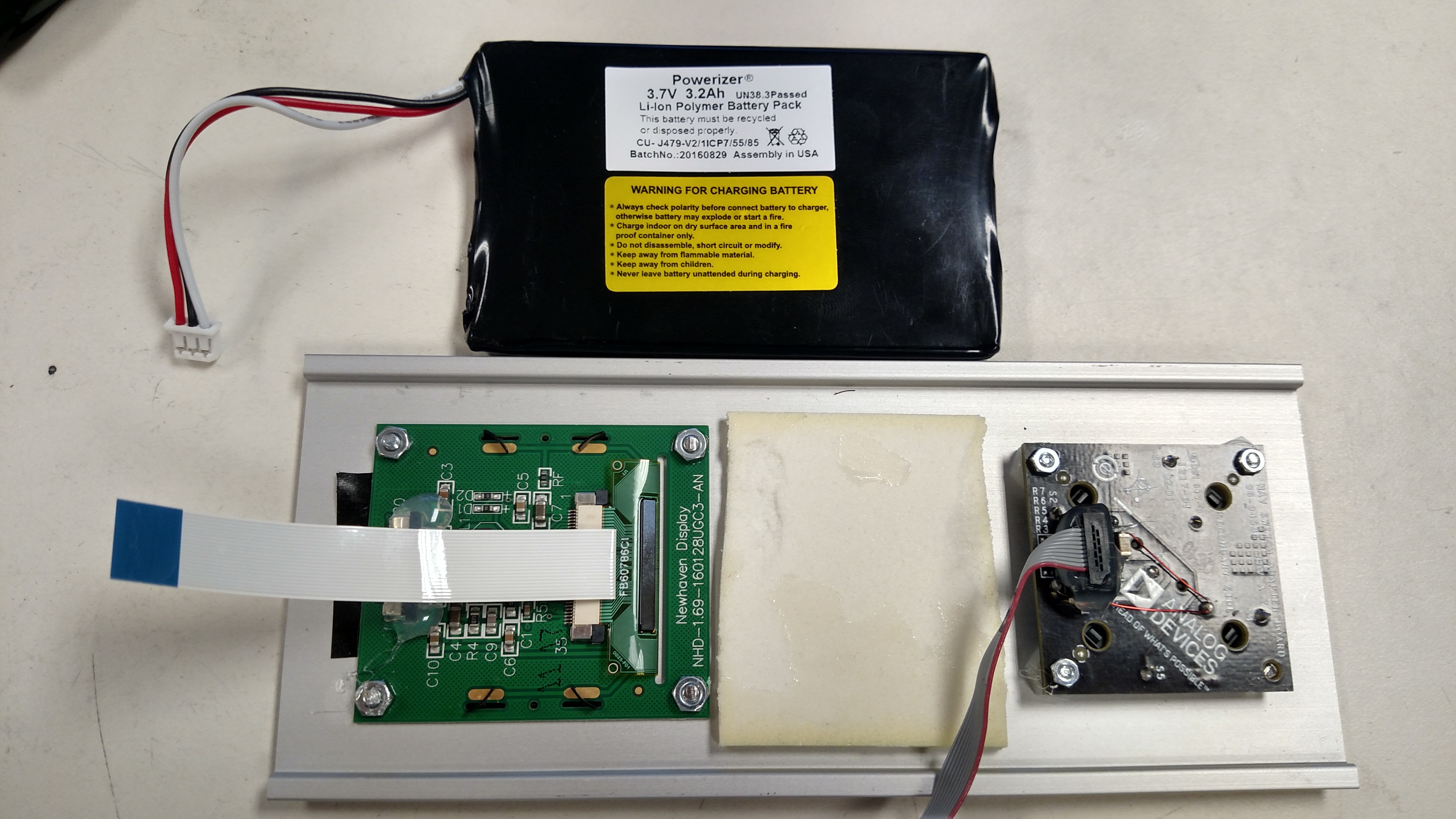
Place 4× M2.5 × 8mm screws through the belly plate. Apply Loctite 242.
Place 4× 908-135 standoffs onto the screws.
Place the Nav Switch PCB into the circular opening with the connector closer to the middle of the belly plate. Attach 4× M2.5 nuts and tighten.
Insert the ribbon cable into the connector on the Nav Switch so it extends towards the battery. Bend the cable towards the red line and pull it out to the left side. Apply hot glue to the connector and a fraction of the cable to secure everything.
Note
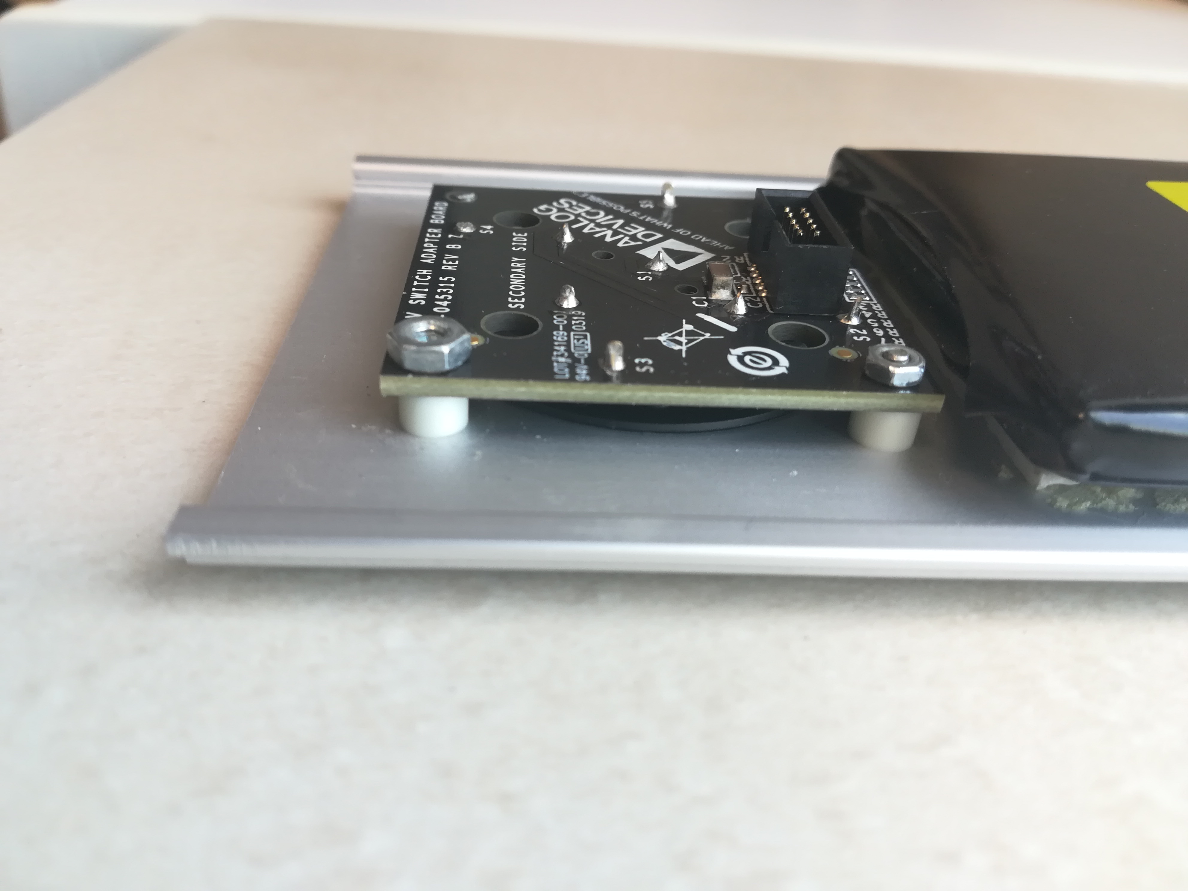
There is a clearance constraint between this cable header and a component on the bottom of the PCB. Glue must be restricted to below the top of the cable header when plugged into the Nav Switch PCB.
Battery Installation
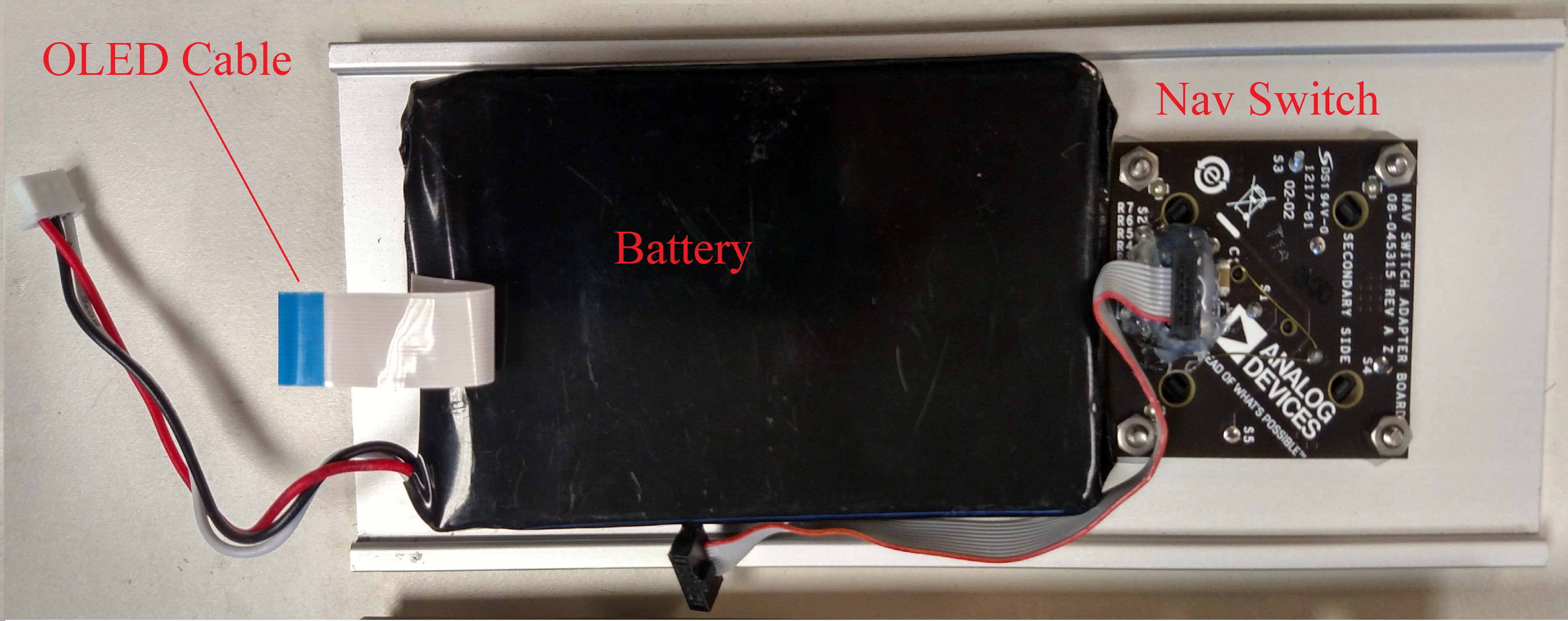
Battery CU-J479-V6: Molex 51065-0300
Clean the area between the two PCBs with a dry cloth.
Cut a 1–1.25 inch piece of double-sided tape, peel off the cover, and place firmly between the PCBs.
Place the battery firmly onto the tape with the yellow and white labels facing away from the belly plate.
Preparing the ADRV936x PCB
Heatsink Installation
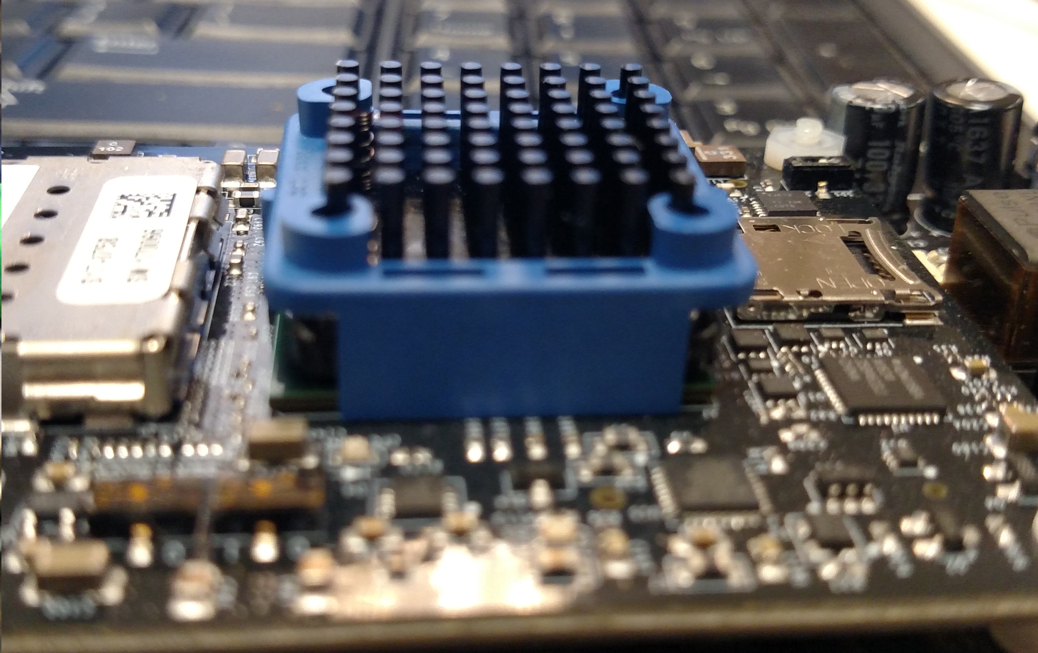
Apply a circle of thermal grease to the protruding portion of the Xilinx FPGA and spread the paste around.
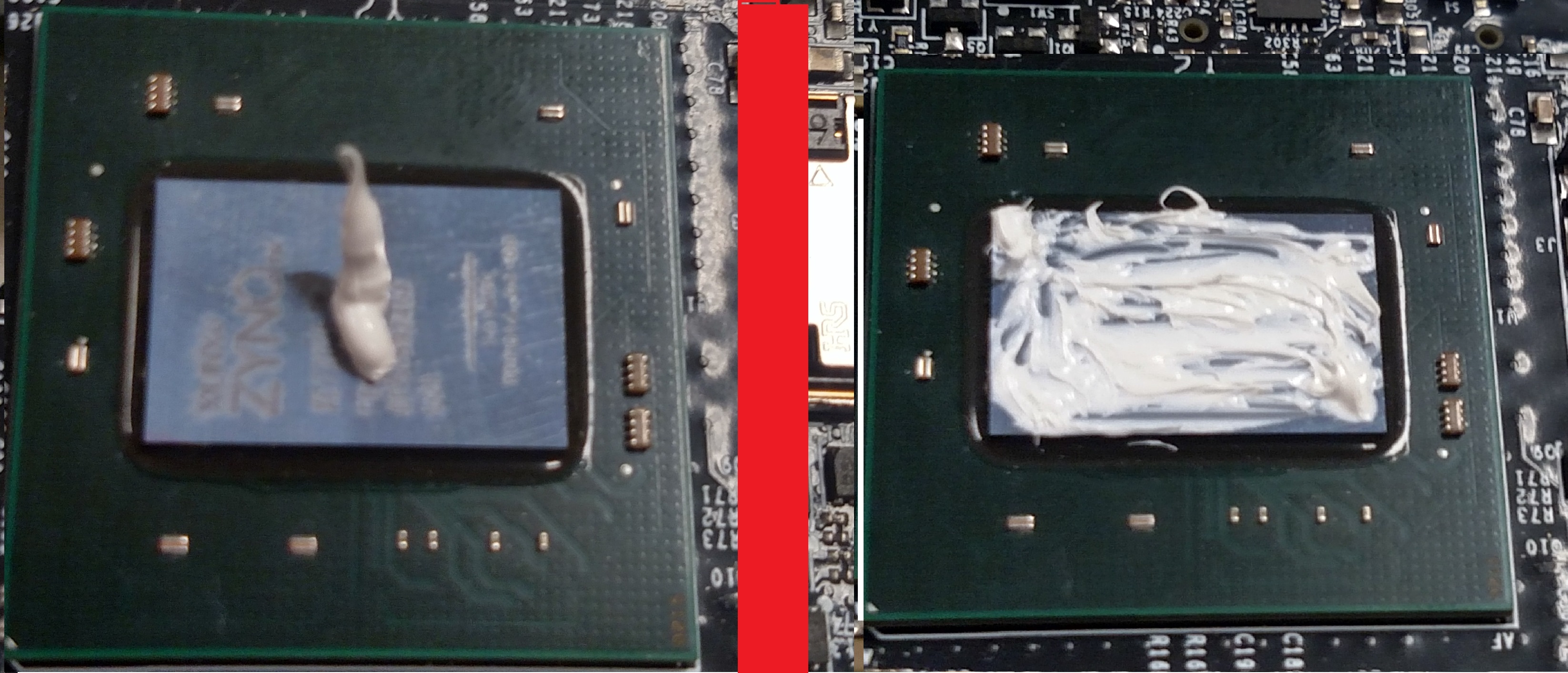
Carefully place the heatsink making sure the plastic frame snaps into place.
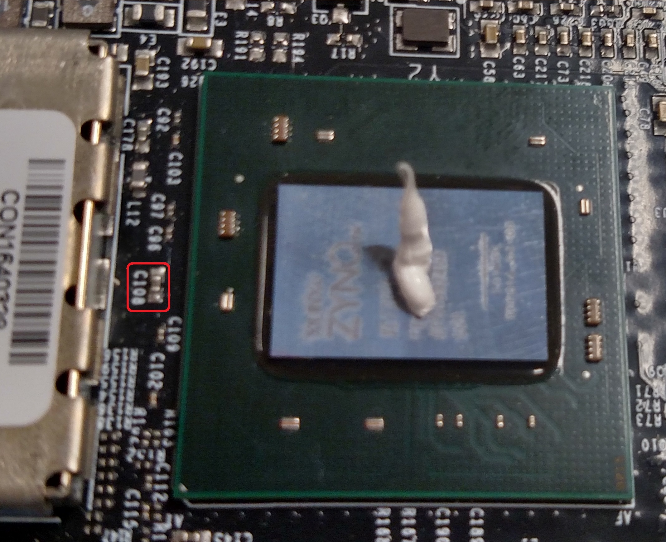
Warning
Be careful of C108. The plastic of the heatsink frame can catch on this component and damage it if too much force is applied.
Boot Switch Configuration
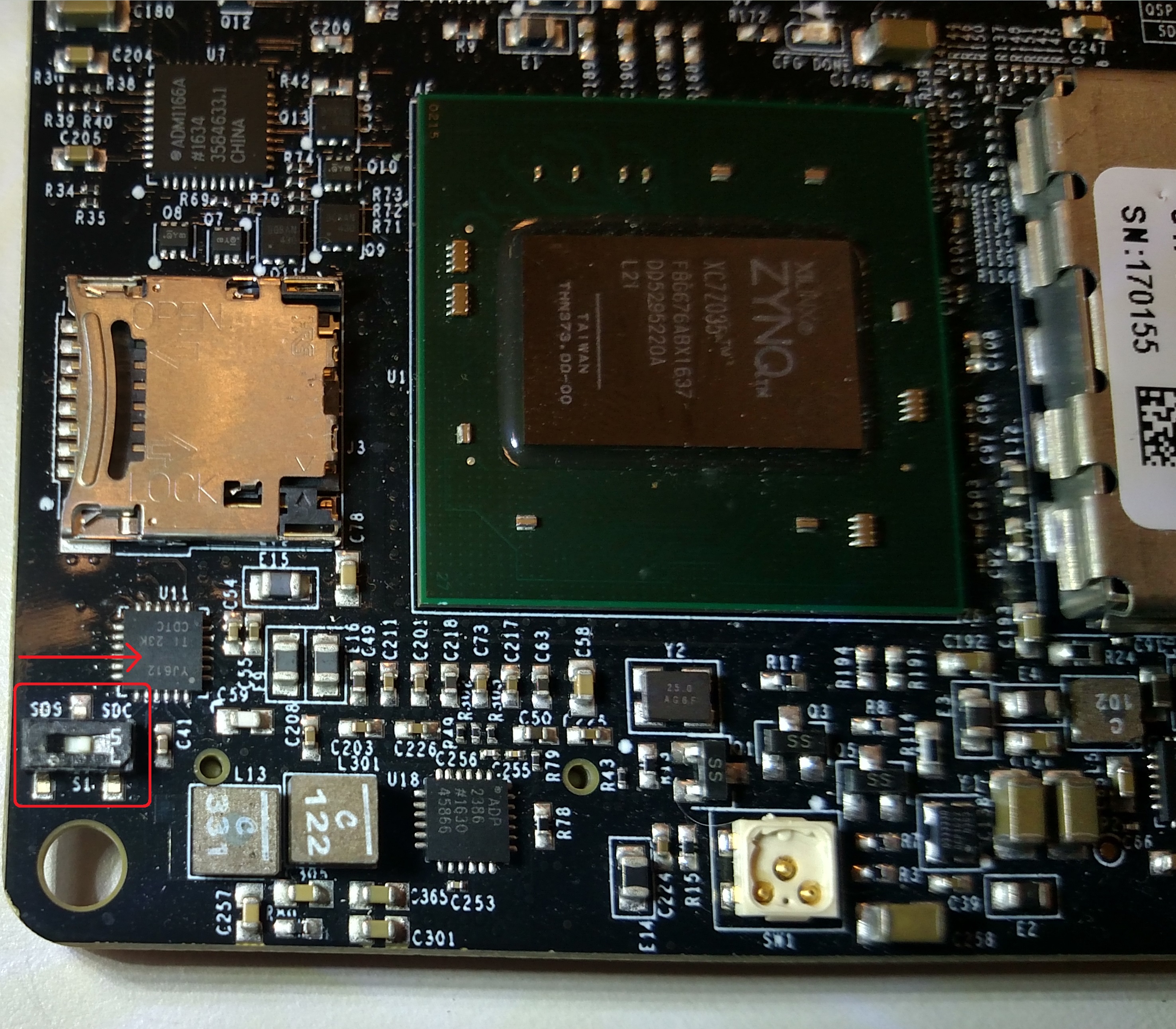
The PCB must boot using the micro SD card connector on the carrier board. Using tweezers or a small screwdriver, move switch S1 into the SDC position (text on either side of the switch indicates the correct orientation).
Connecting the PCBs
Line up the ADRV936x PCB connectors with those on the carrier card. The boards will only mate in one orientation — rotate 180° if it does not fit. Do not force the connection; little force is required when properly aligned.
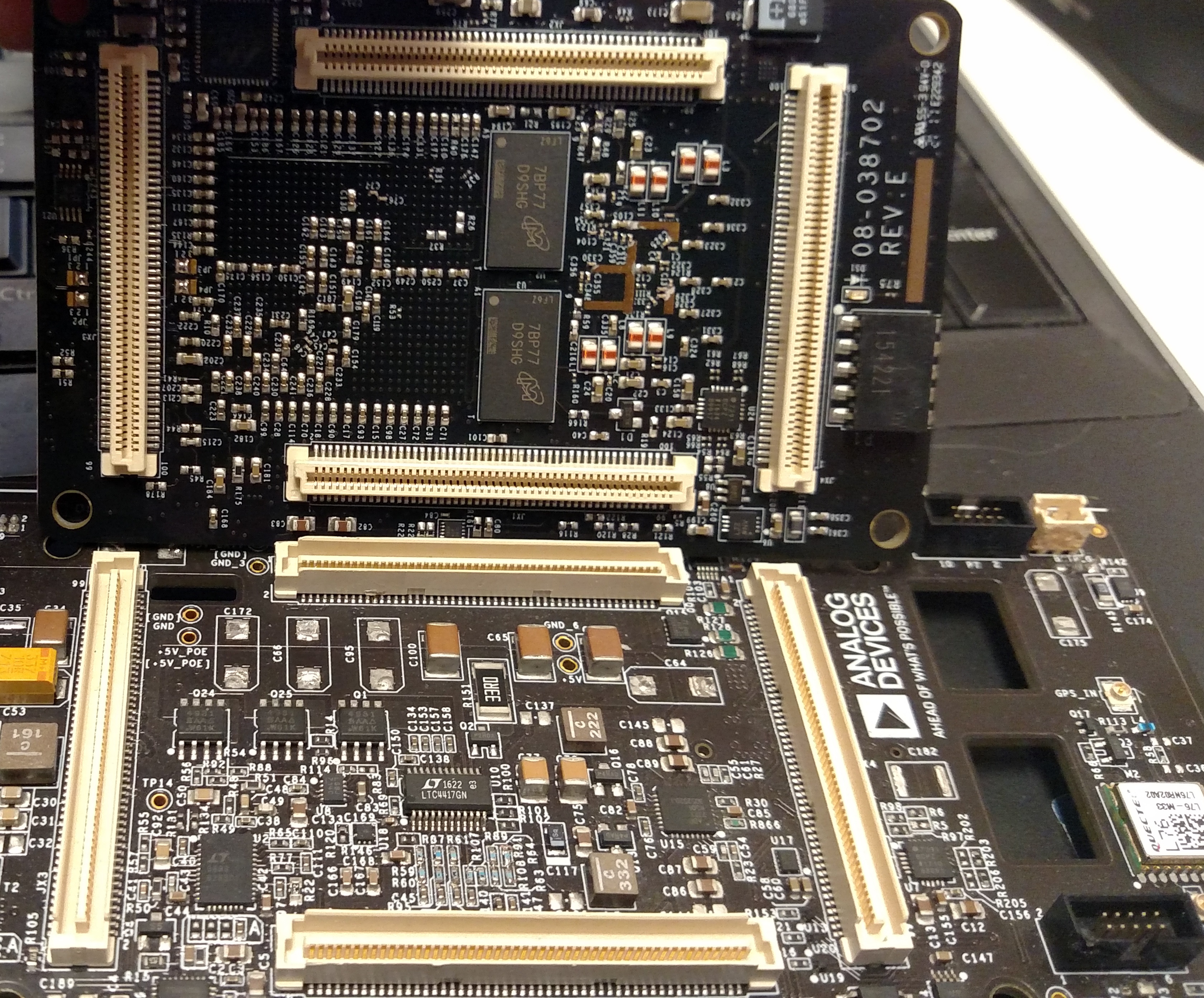
The image below shows the cards before being pressed together. Notice the gaps at the edges of the connectors.
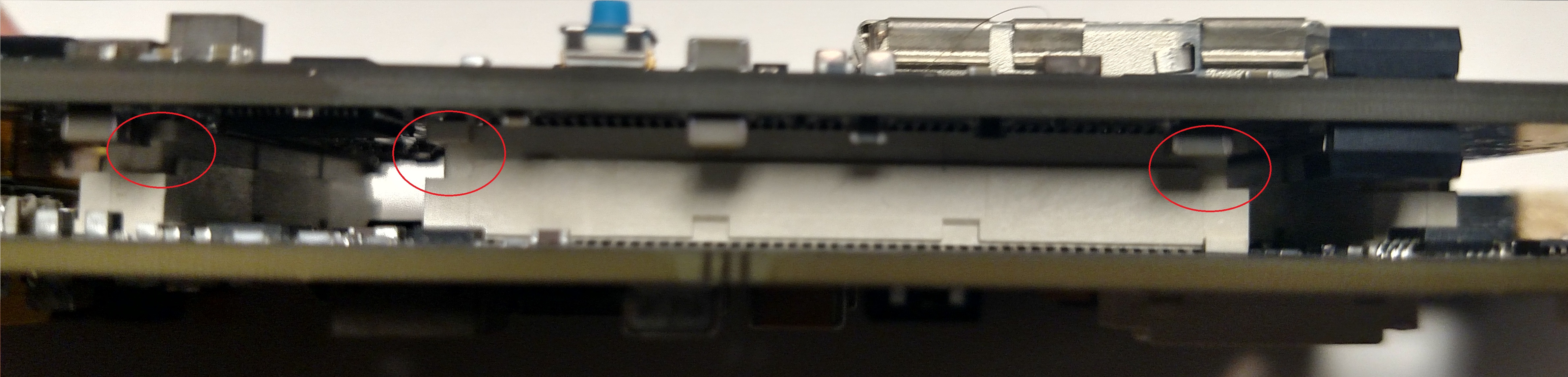
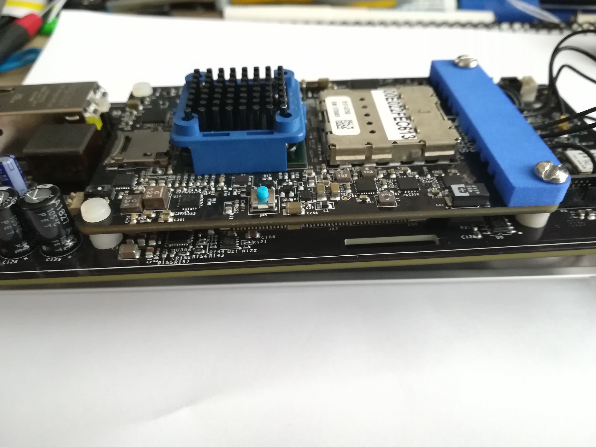
The following image shows the cards properly mated.
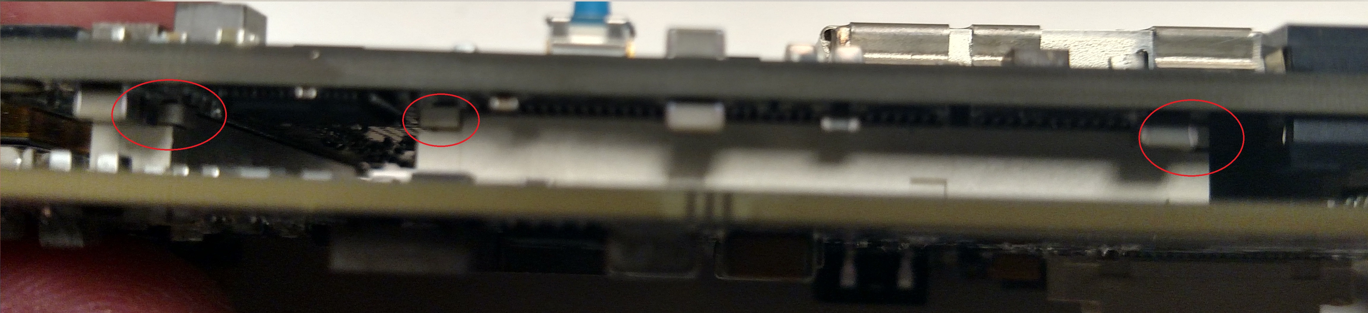
Make sure to press all four corners to ensure a solid connection.
Connecting the RF cables
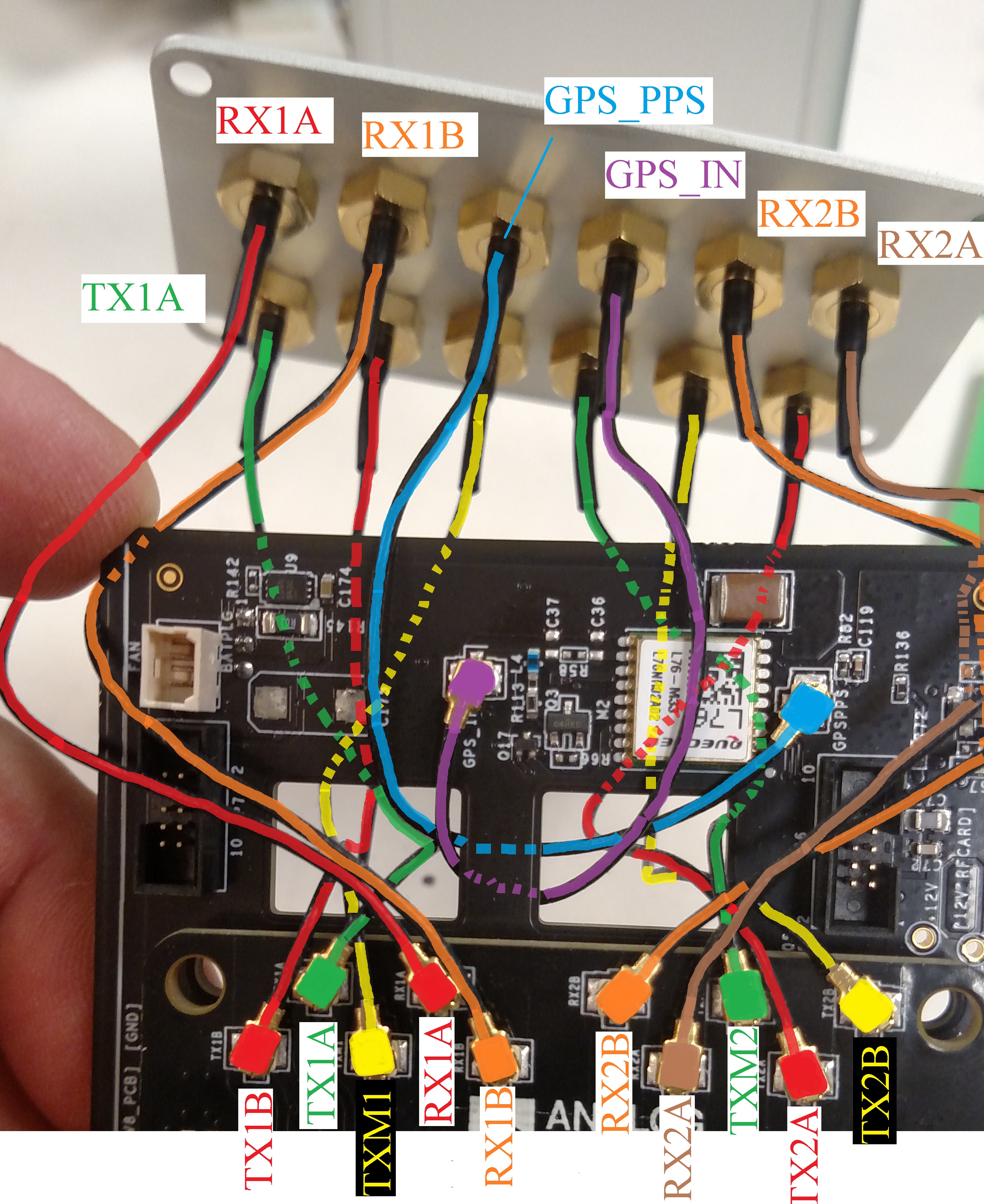
Connecting 12 U.FL-to-SMA cables to the pair of PCBs and face plate of the box is a challenging but critical step. Take care to make the correct connections and route the cables carefully.
Fasten all cables to the face plate THEN connect them to the PCBs. Hold the connector in place when tightening the nut to avoid damaging the face plate.
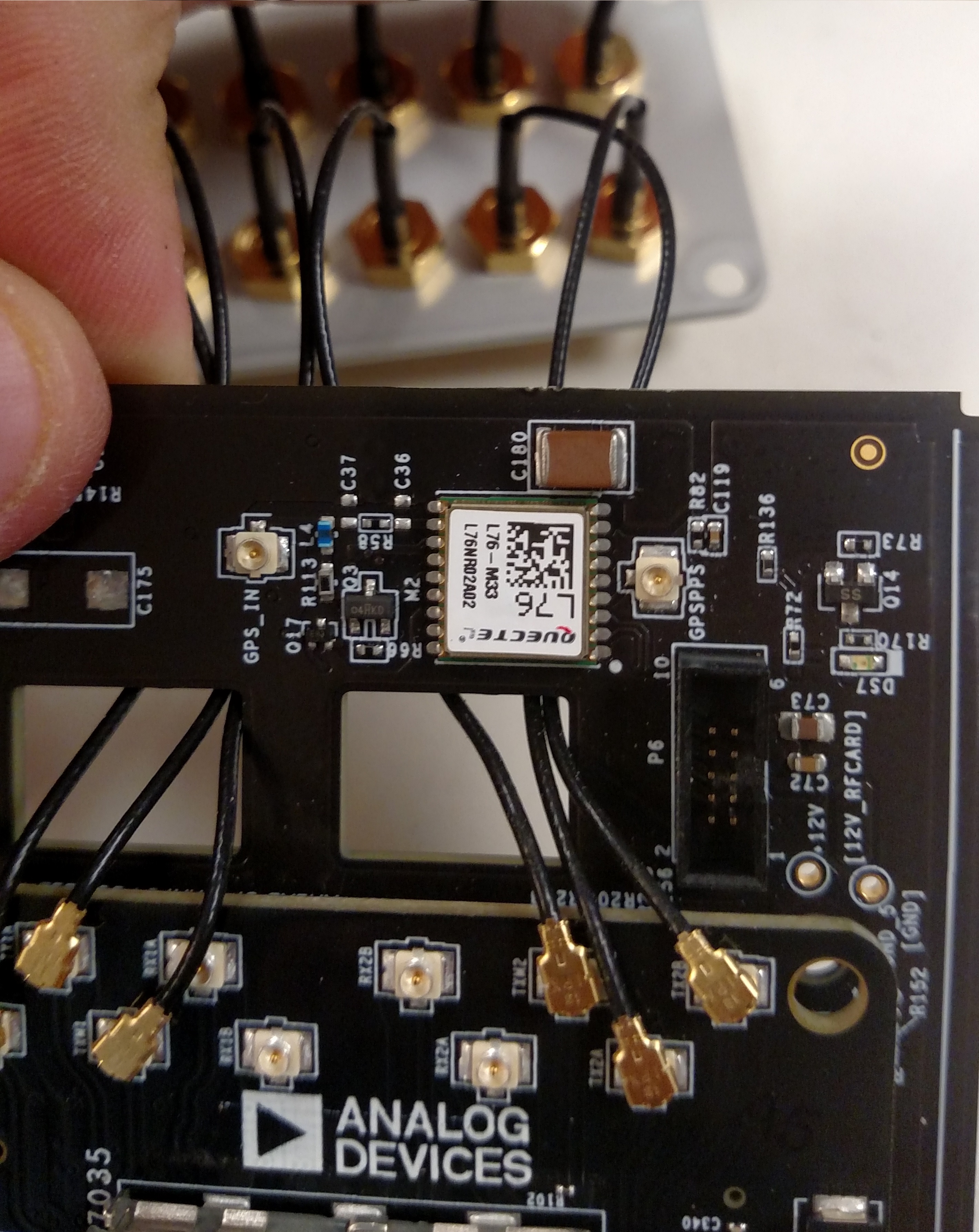
Each cable connects to a specific connector on the PCB. Firmly connect one cable before moving on to the next.
All TX cables go through the hole in the PCB closest to them.
None of the RX cables go through the PCB holes.
GPS cables go through both holes.
Securing the RF Cables
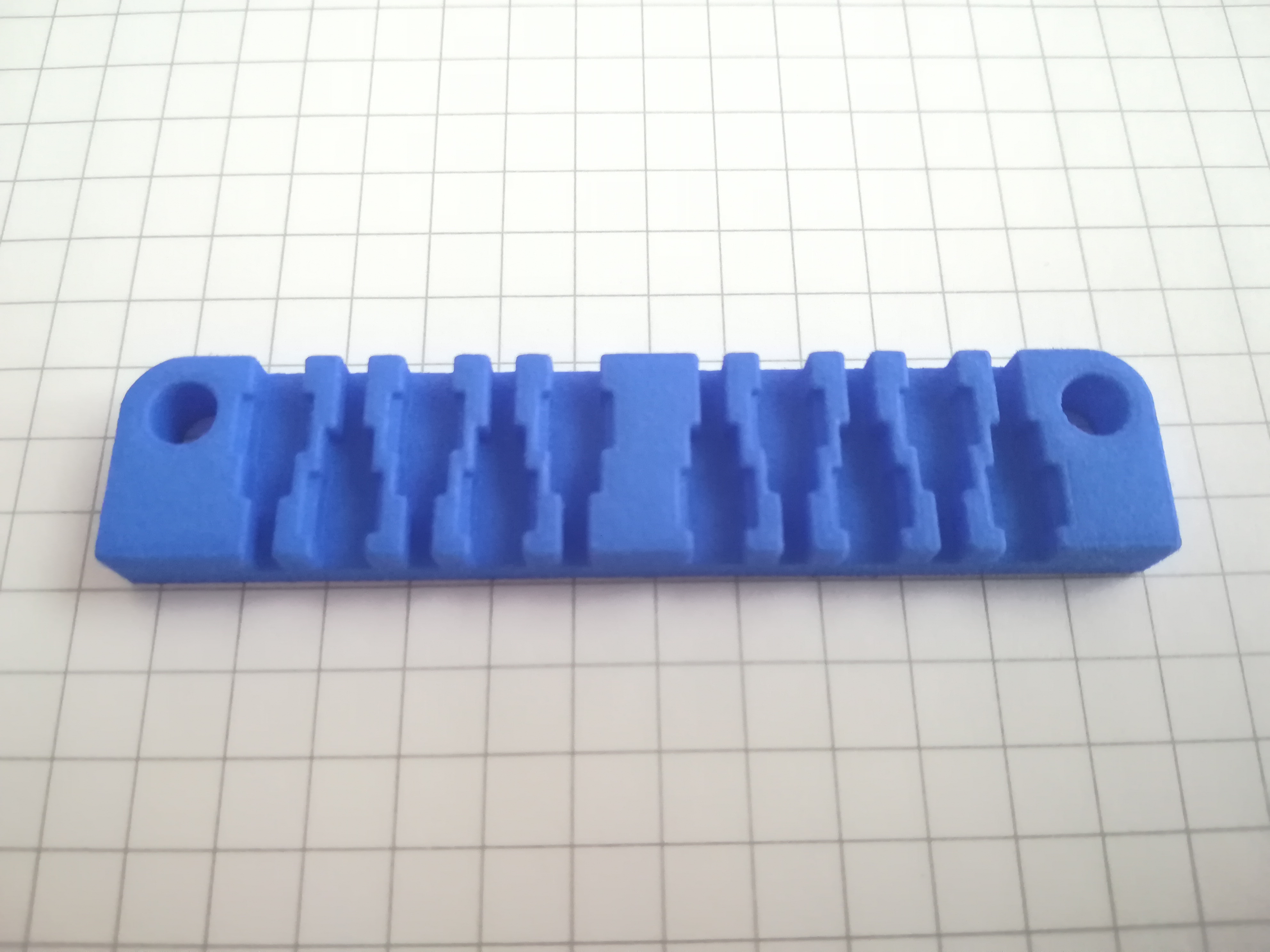
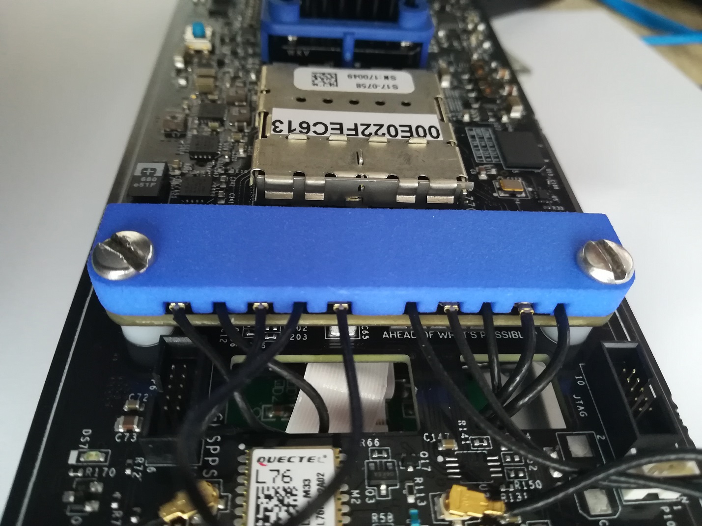
A 3D-printed cable brace holds all connectors and cables in place, protecting the delicate U.FL connectors from movement or accidental damage.
Make sure each U.FL connector is perpendicular to the edge of the board.
Gently place the brace down on top of the cables and PCB, aligning the holes of the brace with the holes of the PCB.

Securing the PCBs
Place 4× 5mm nylon spacers between the PCBs, aligned with the corner holes of the SOM PCB.
Insert 2× #6-32 metal screws on the cable brace side. Apply Loctite 242. Secure with metal hex nuts. Do not over-tighten.
Insert 2× #6-32 nylon screws in the other two mounting holes. Apply Loctite 242. Secure with nylon hex nuts. Do not over-tighten.
Once these steps are complete, begin the radio Partial Assembly Test.
Stage 2 — Full Assembly
Body Plate
IMU Assembly
Connect the IMU to the adapter PCB, making sure to properly align the header with the receptacle.
Plug the ribbon cable into the adapter PCB.
Insert screws into the body plate. Place the IMU into the screws with the adapter PCB away from the case.
Add Loctite to the screws. Add nuts and tighten according to the ADIS16460 instructions (a torque wrench is required).
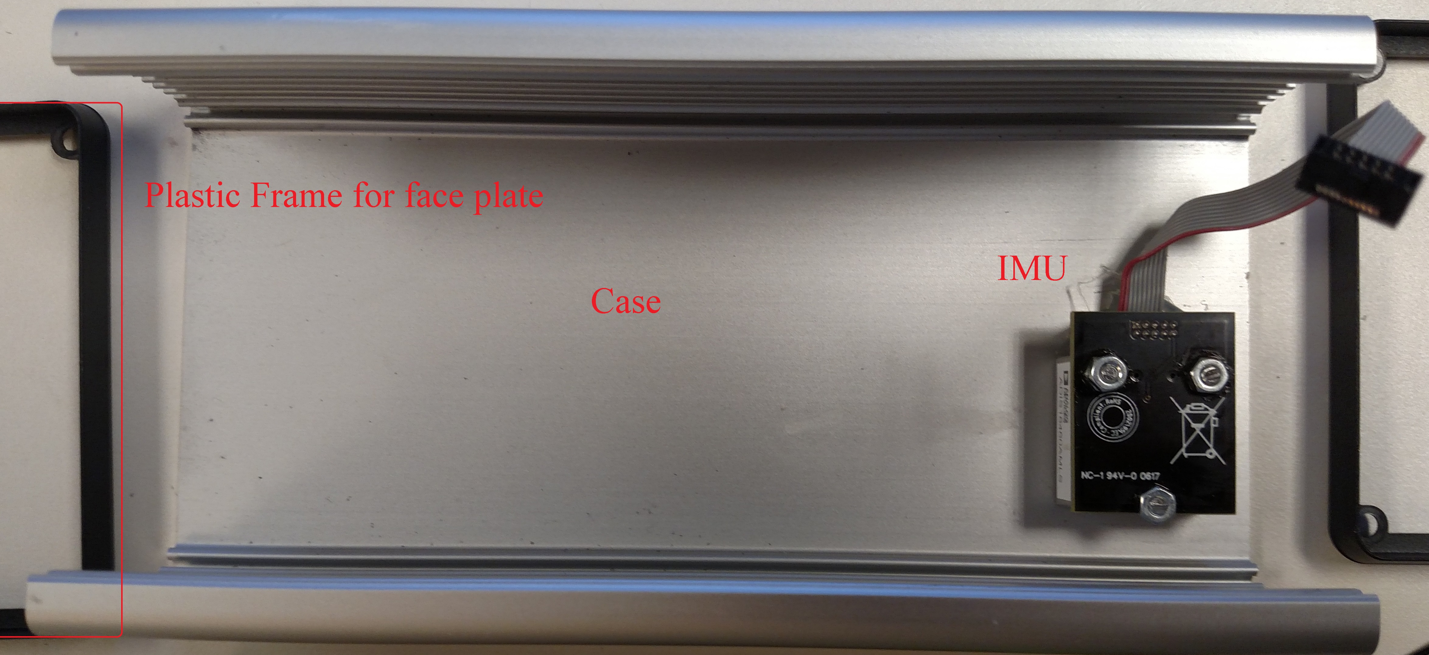
Apply hot glue to the connector.
Cutting a Slot for the JTAG Adapter Cable
Note
This procedure needs to be performed on only half of the boxes.
Using a table saw, cut a 1.25” opening down the second shelf. This allows the JTAG Adapter cable to protrude from the case. The JTAG adapter cable will be added AFTER the PCBs are inserted.
Inserting the PCBs
Lay both units on the table.
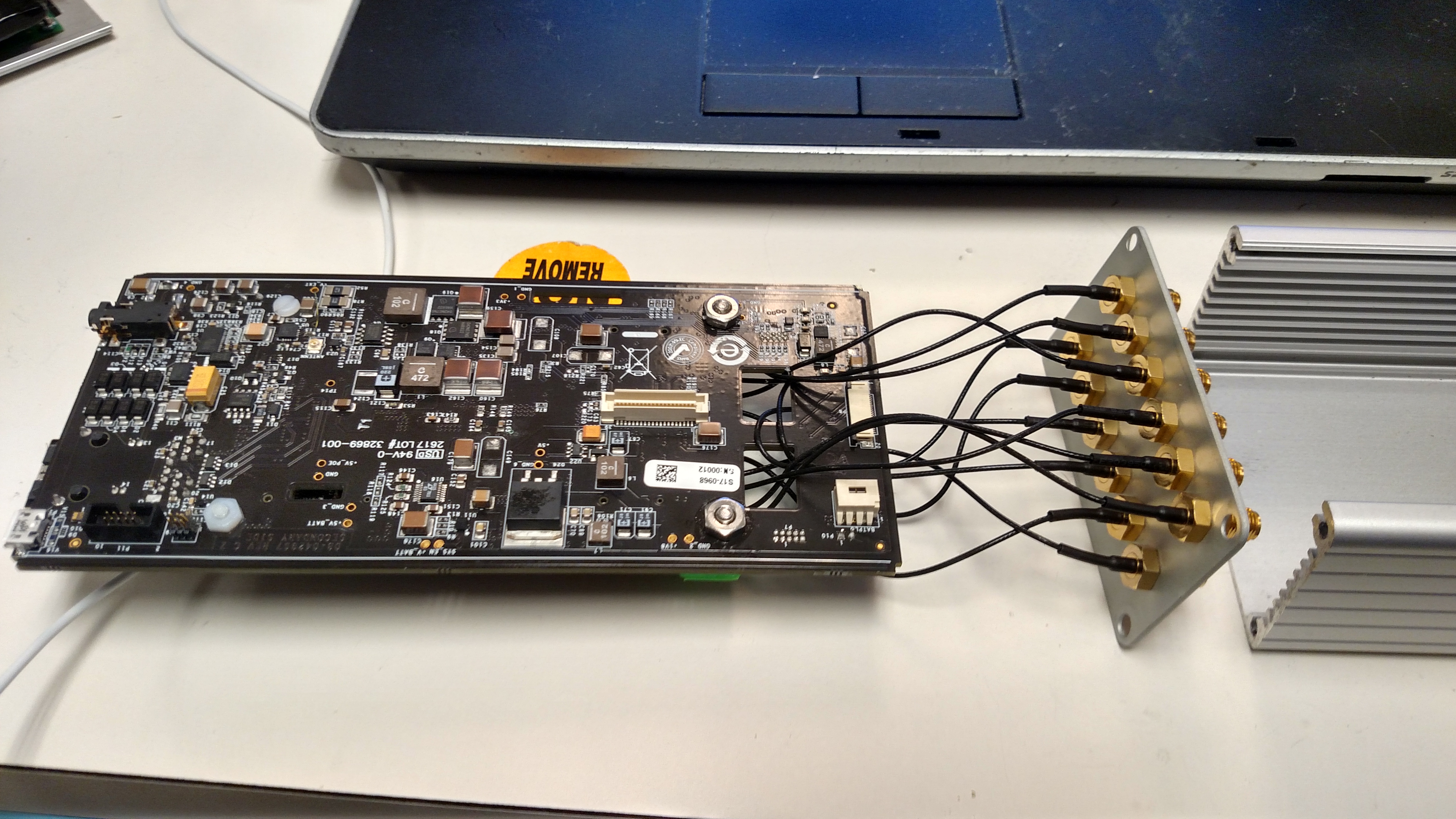
Gently pull the face plate and cables above the PCB.
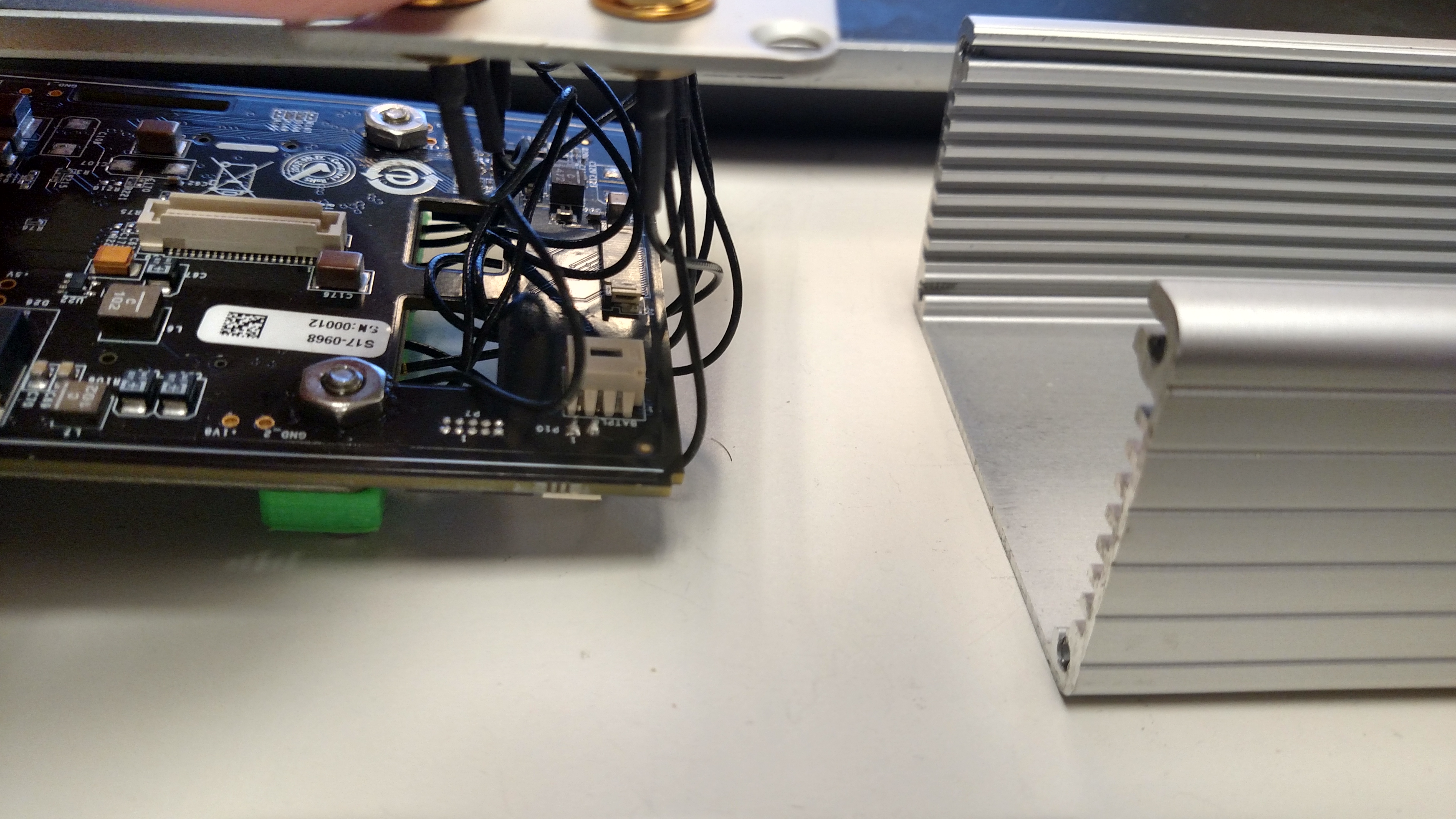
All cables must protrude past the edge of the PCB so they do not get stuck between the PCB and the case.
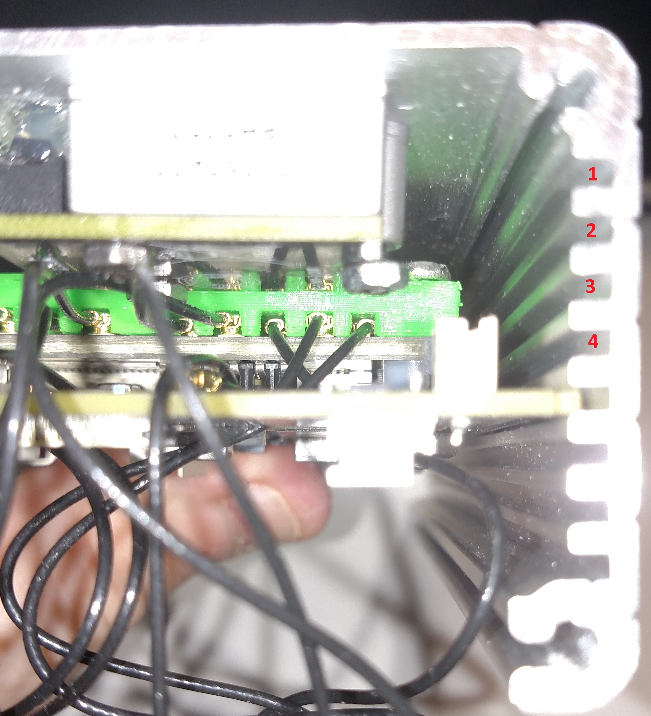
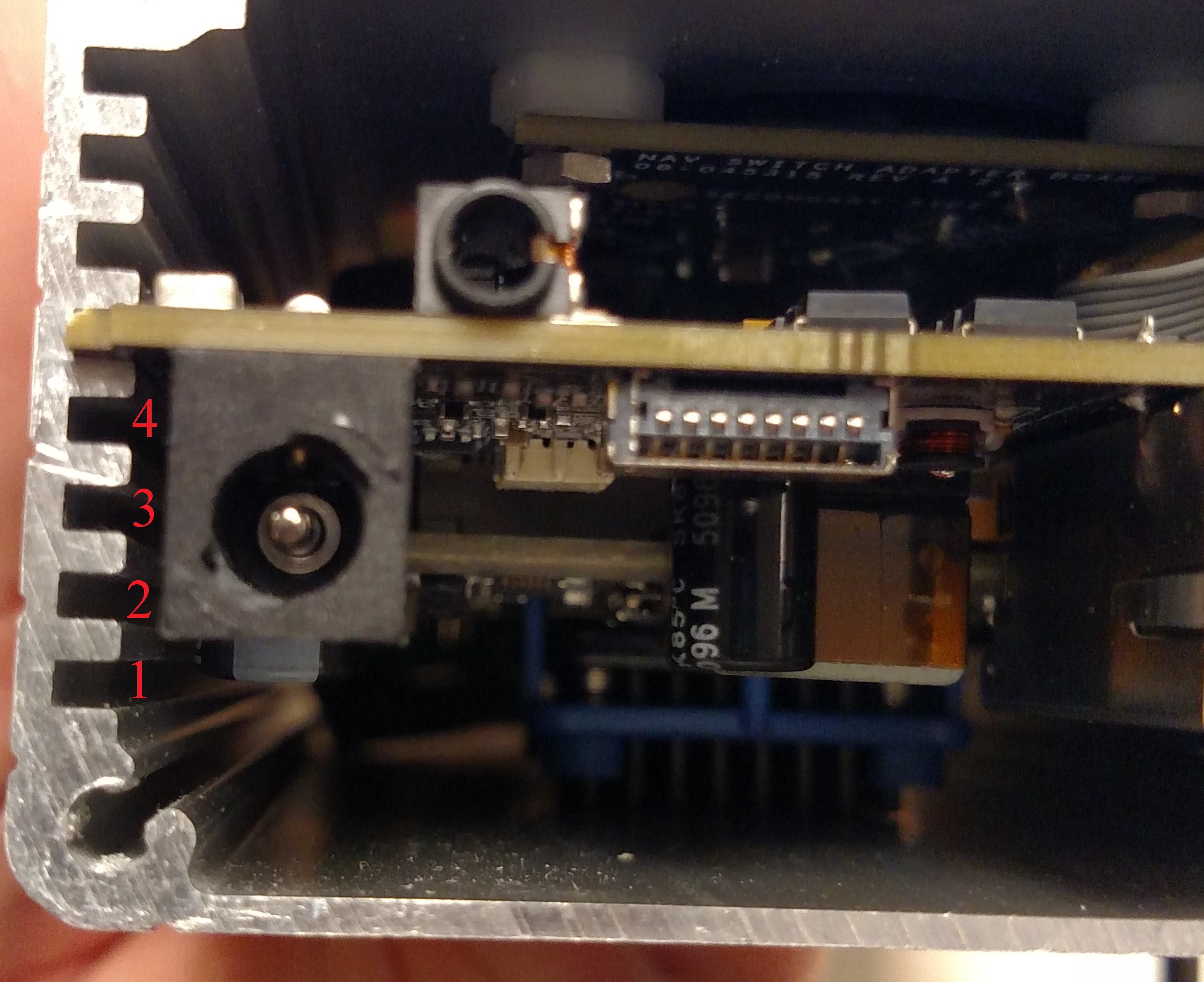
There should be 4 empty rows on the side of the case, with the PCB slotting into the 5th row from the bottom.
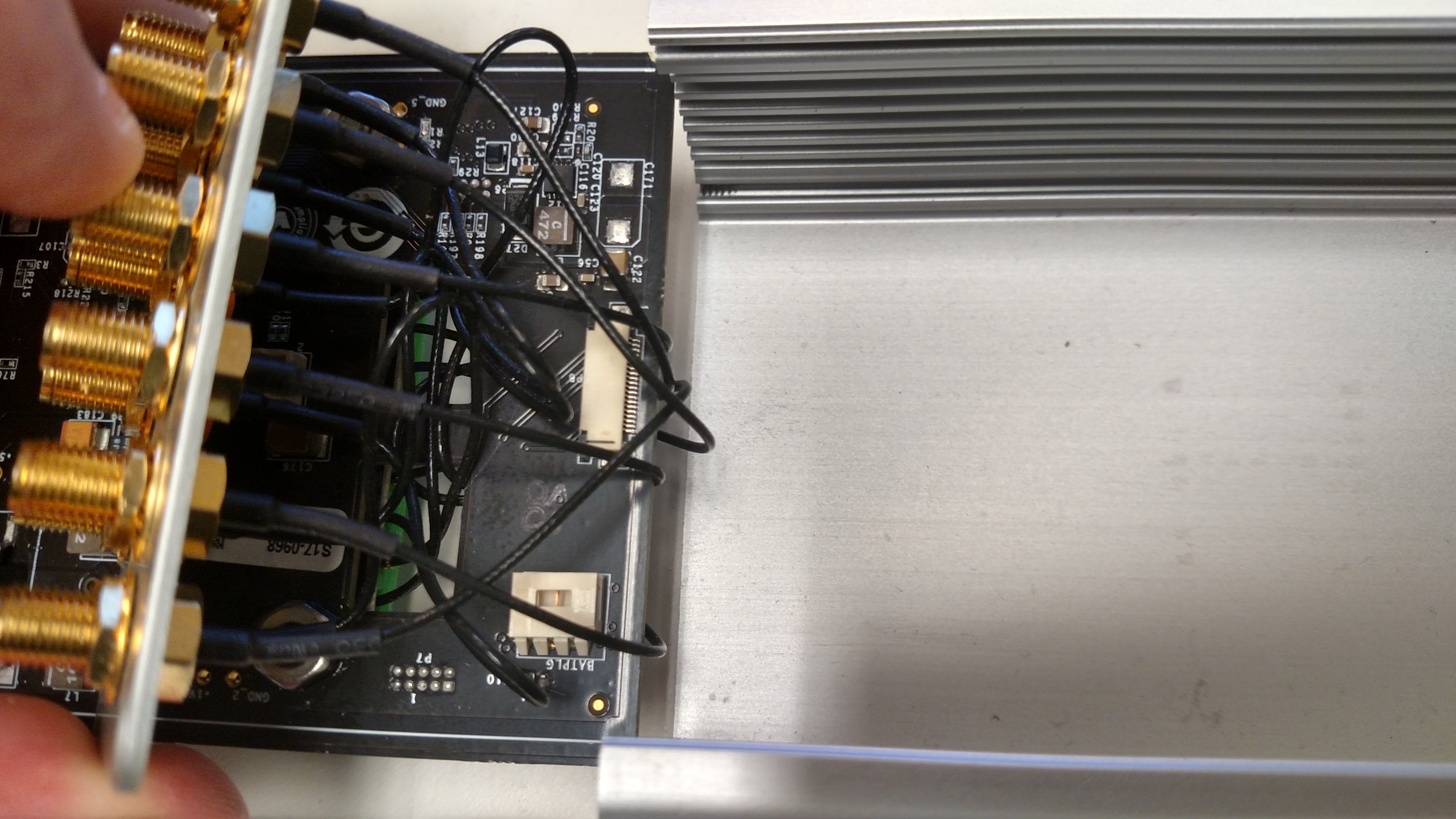
Keep the cables and face plate from being caught between the side of the box and the PCB.
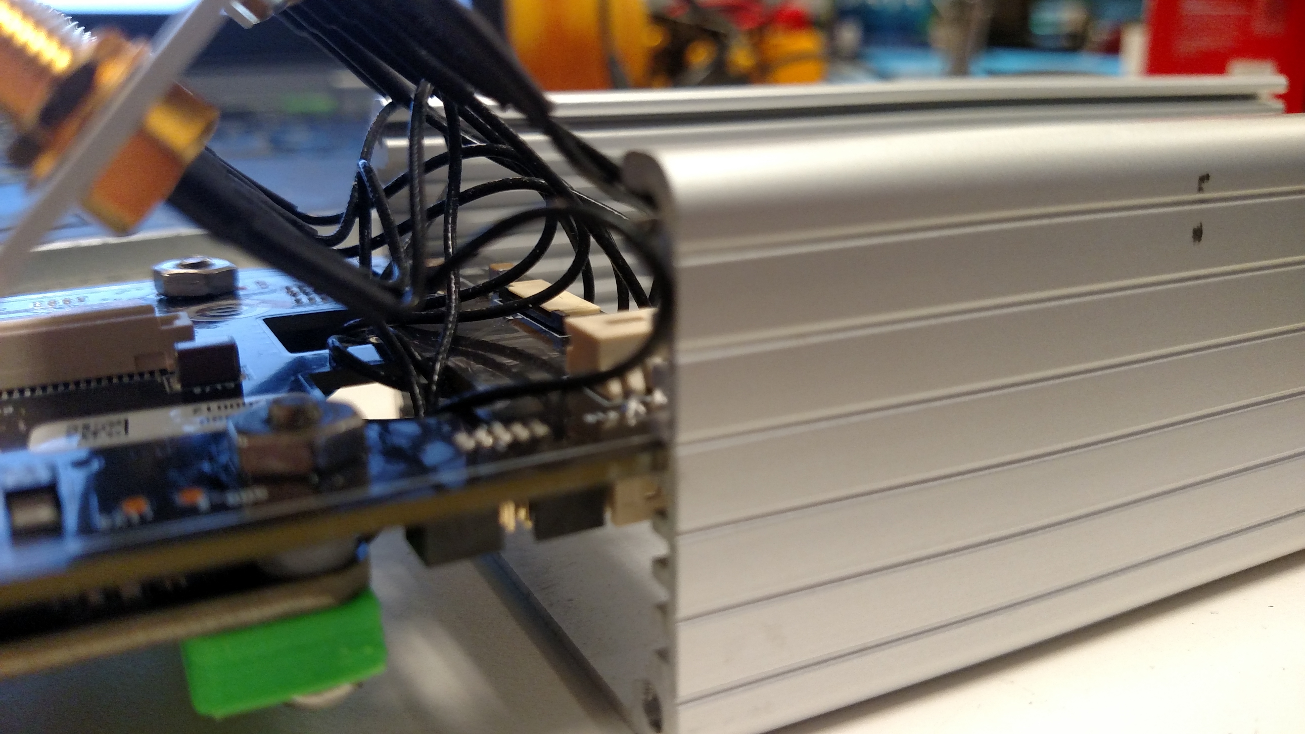
The FPGA is intended to make contact with the metal case. Flex the case slightly if needed for the FPGA to fit.
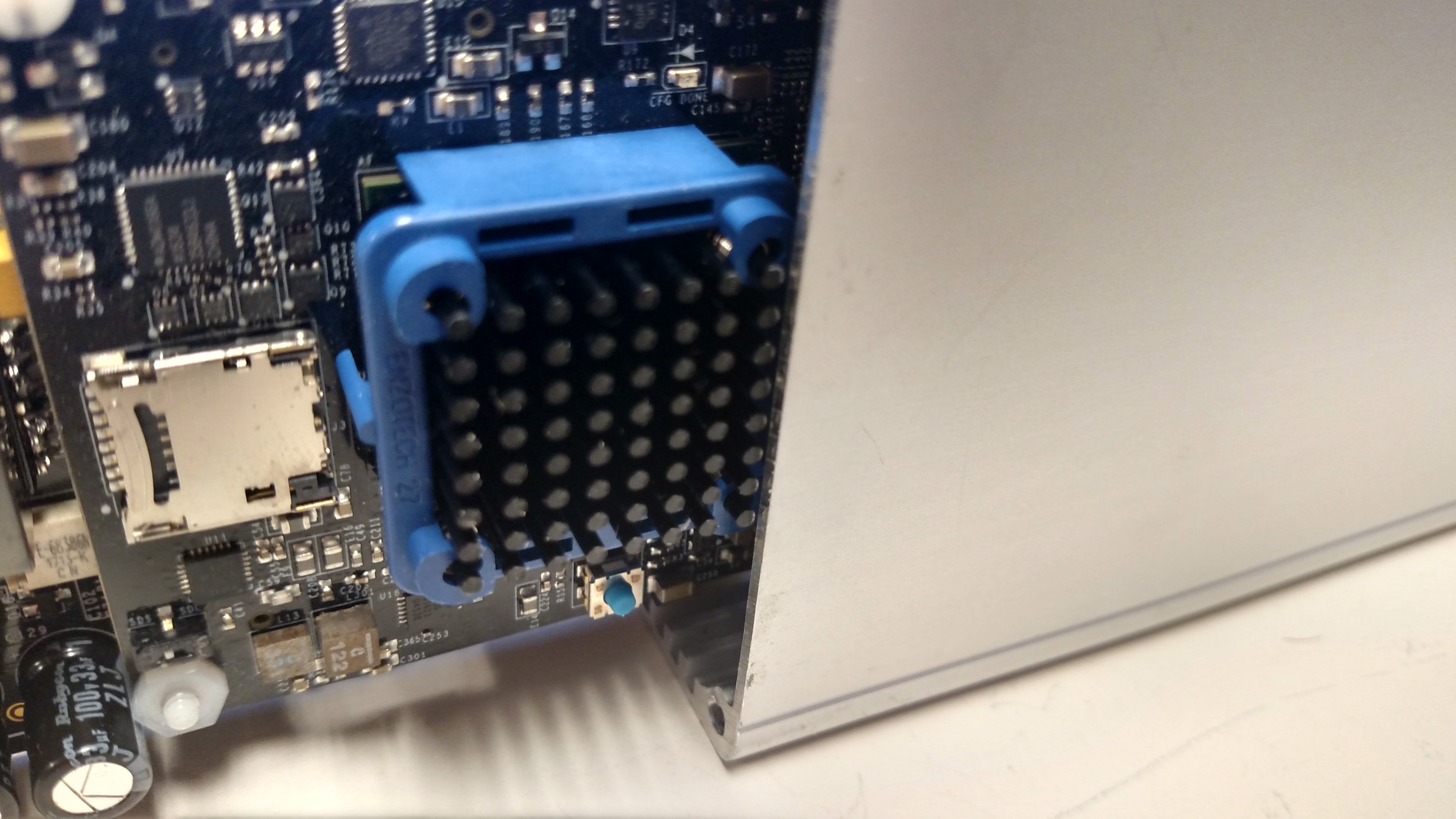
Make sure none of the U.FL-to-SMA cables are caught between the plastic and the IMU adapter PCB.
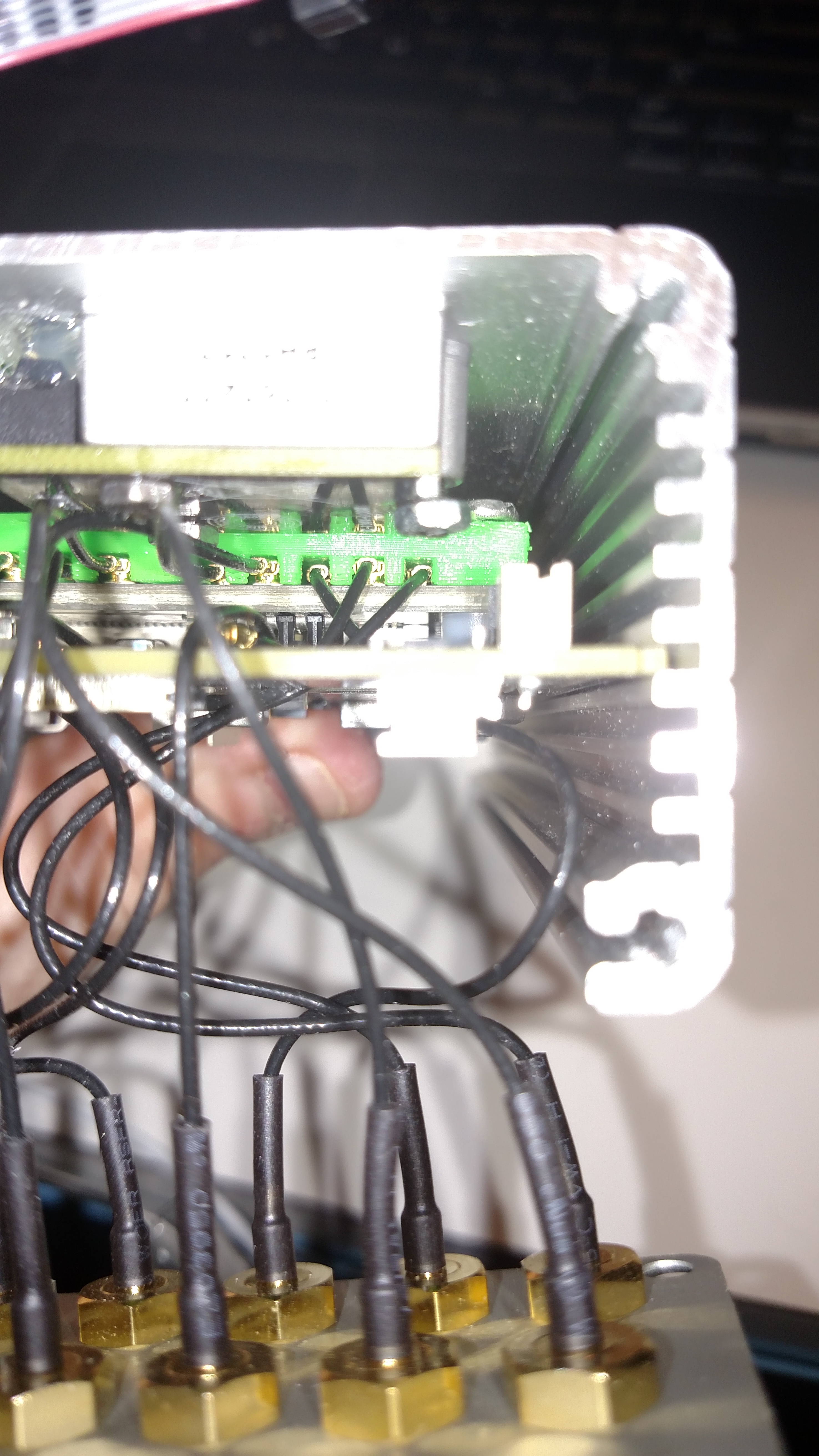
Using tweezers, connect the JTAG Adapter Cable so it protrudes from the opening cut into the box. Apply hot glue to the cable so it does not come loose.
Inserting the Belly Plate
Flip the unit over so the flat surface is down. The belly plate slides into the outermost slot.
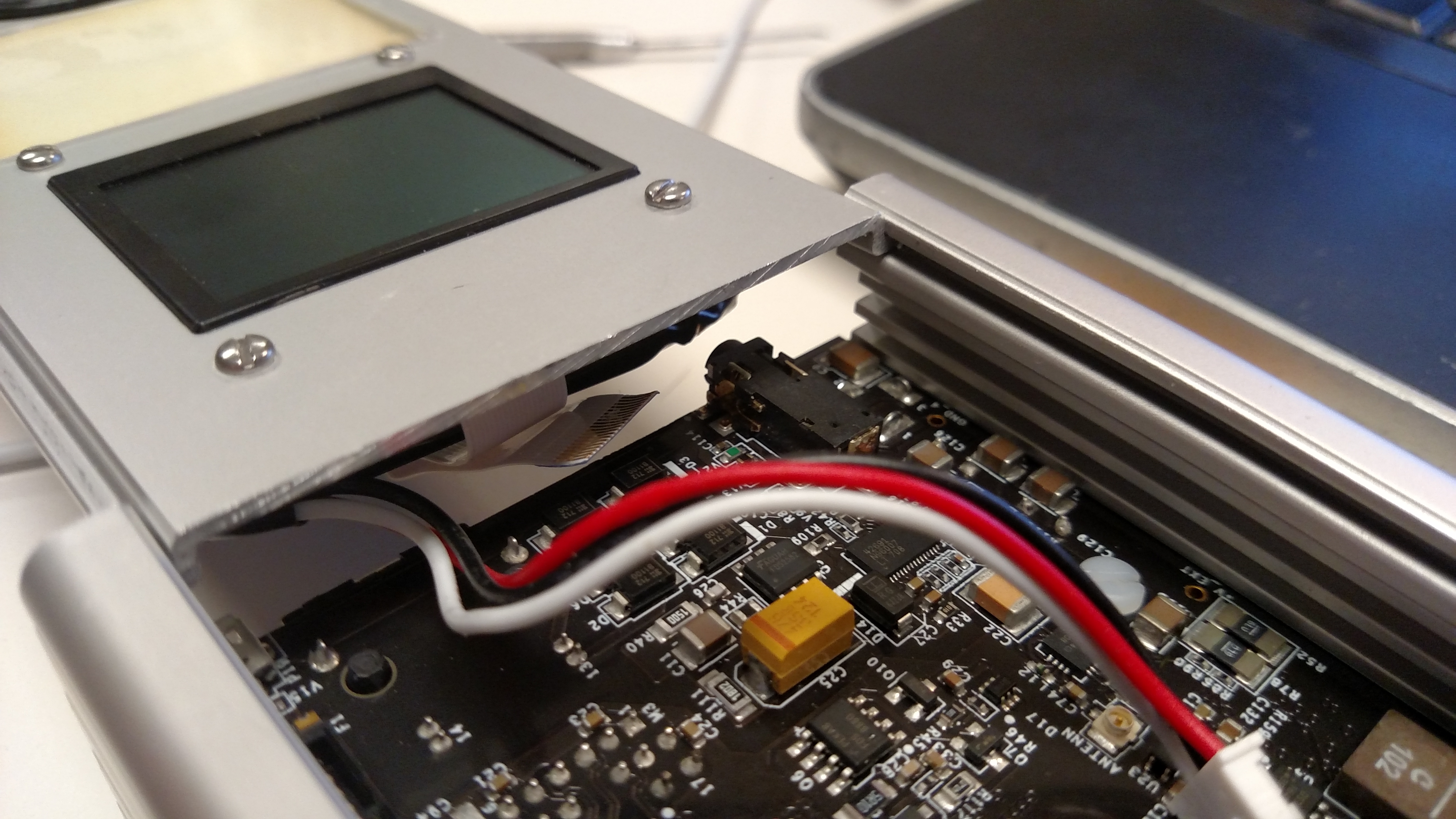
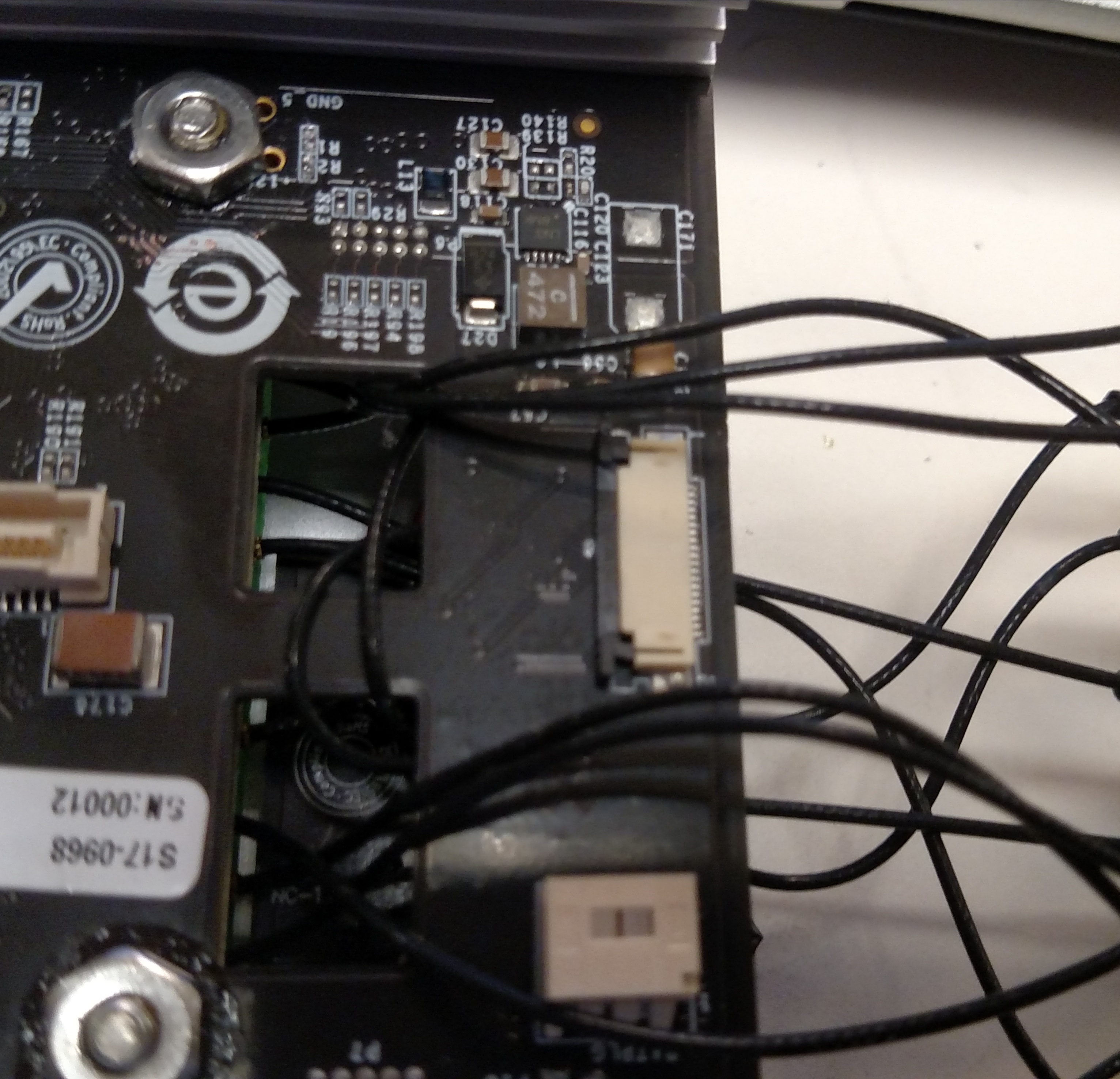
Keep the OLED cable, battery cable, and navigation switch cable from catching on anything. A small screwdriver or tweezers will help with manipulating the cables.
Make sure the OLED connector on the carrier card is open (plastic frame pulled gently away from the connector).
Insert the cable into the connector and close the black plastic to secure it.
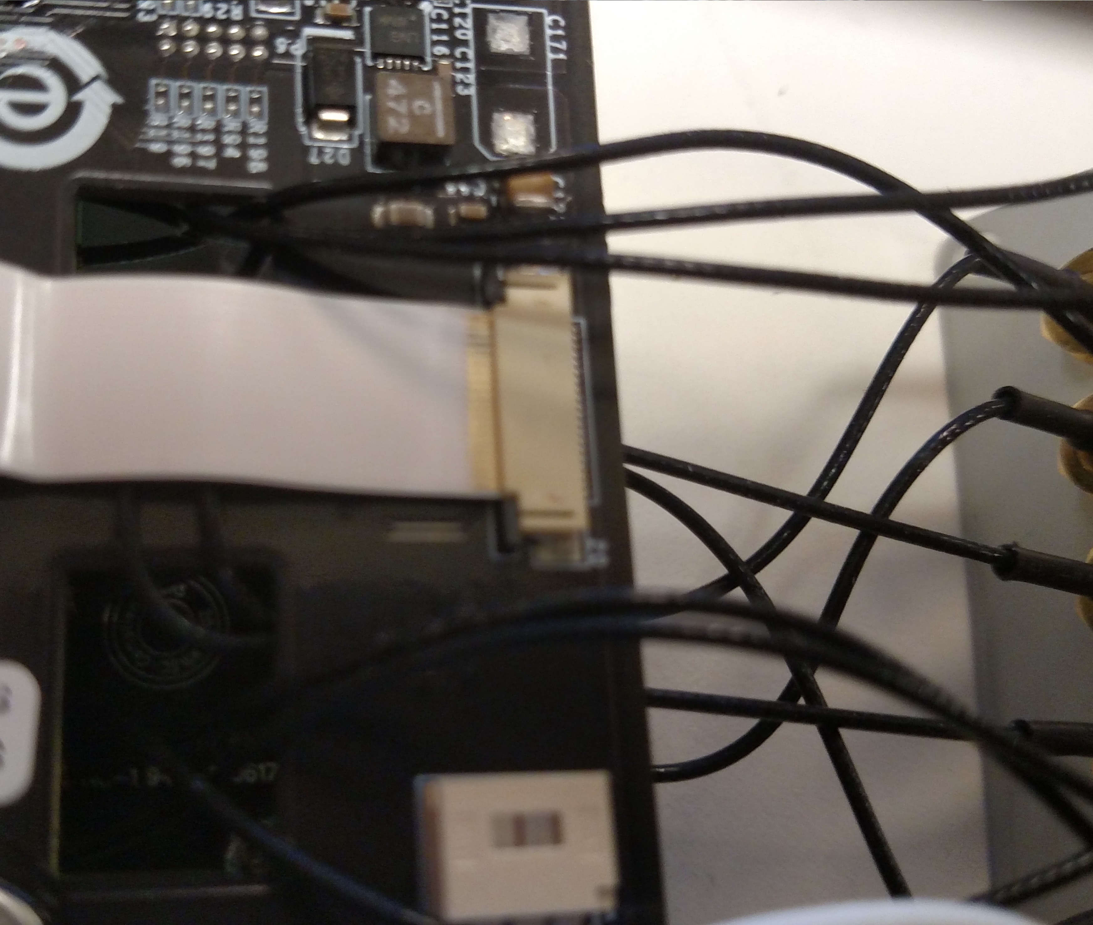
Add hot glue to the connector and cable so any force is applied to the glue and not the connector itself.
Connect the battery cable to the battery plug.
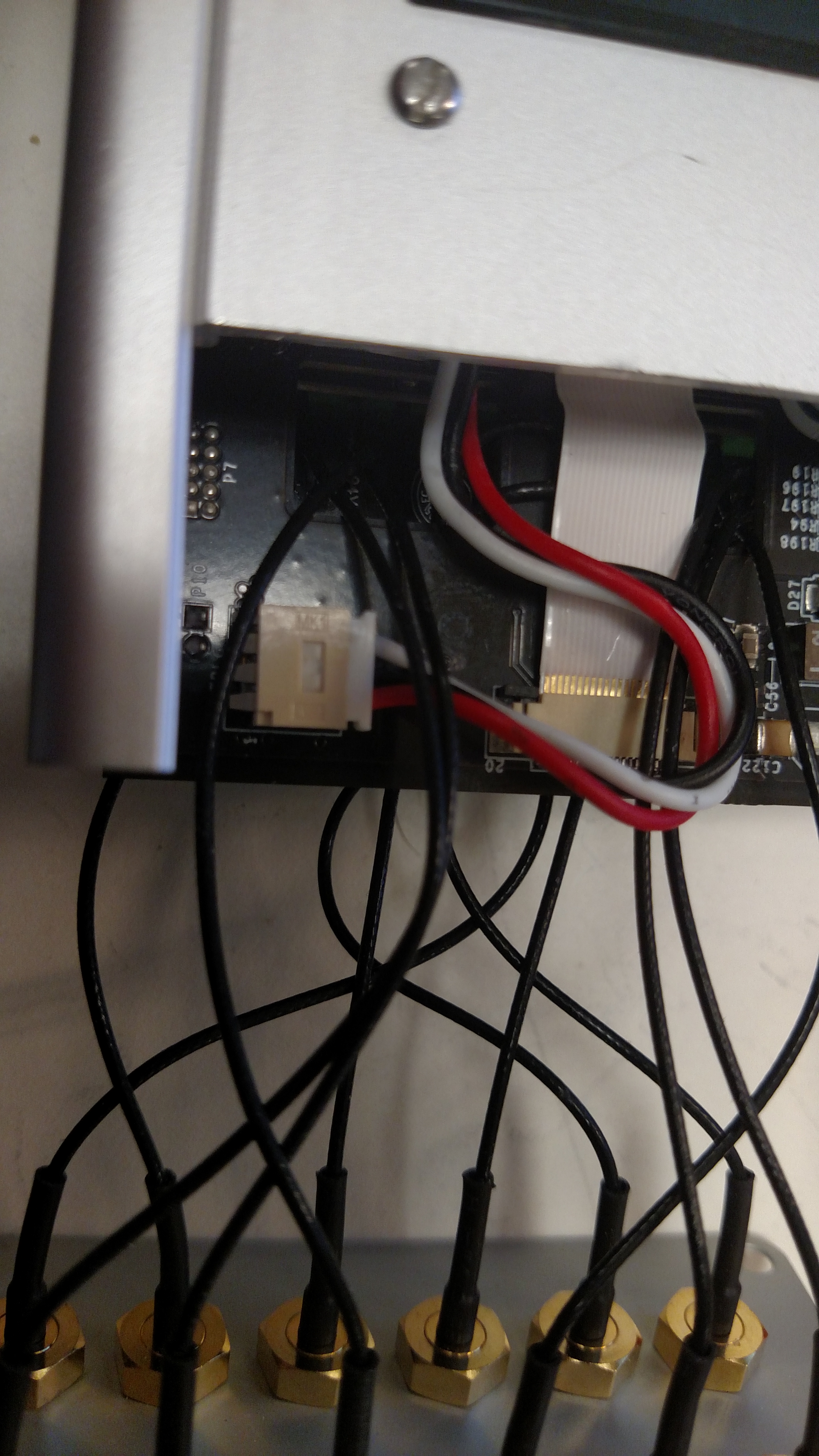
Slide the belly plate so it is flush with either end of the box.
Connecting the IMU
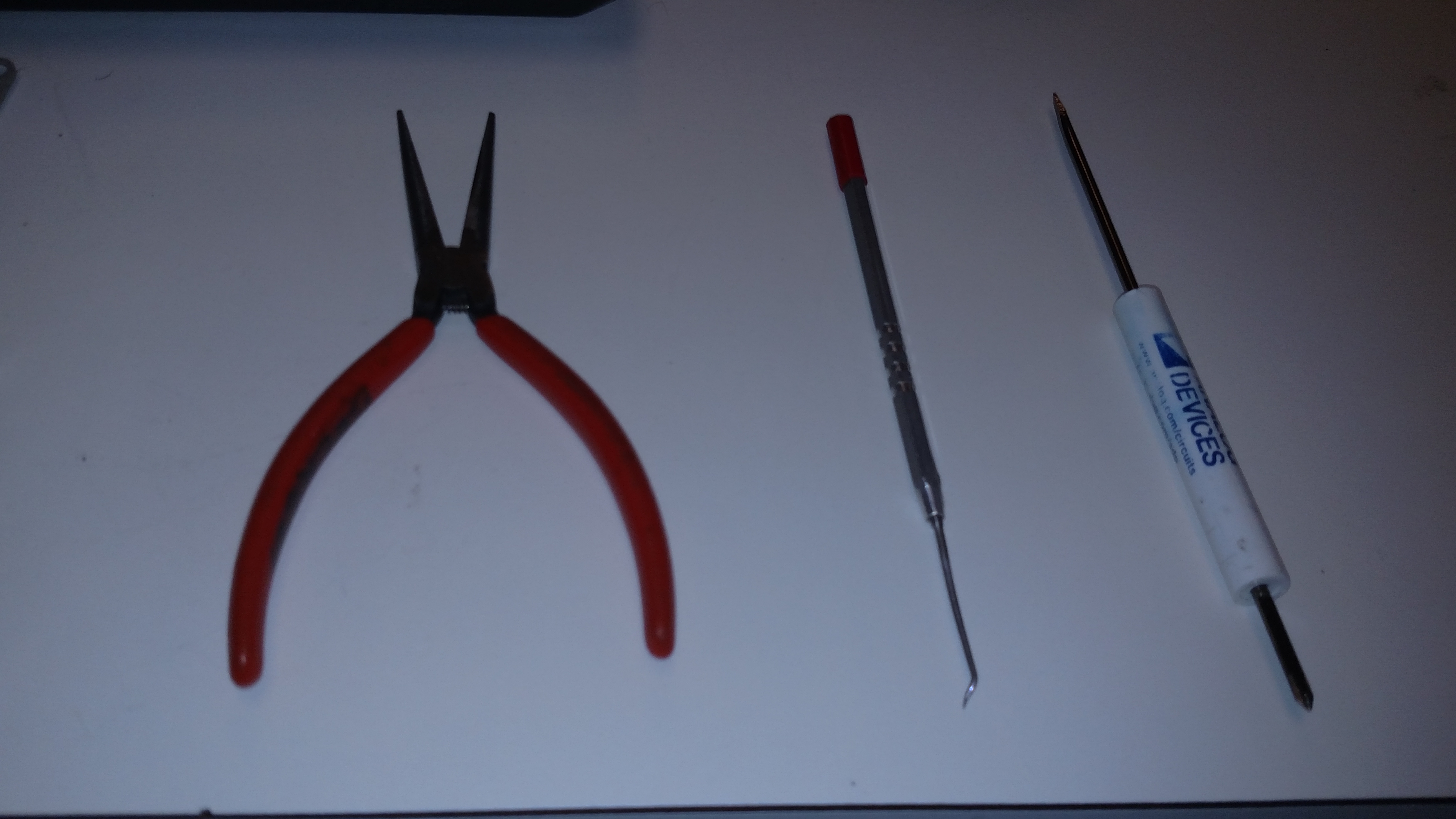
Using tweezers or pliers, grab the IMU cable and gently push it into the connector.
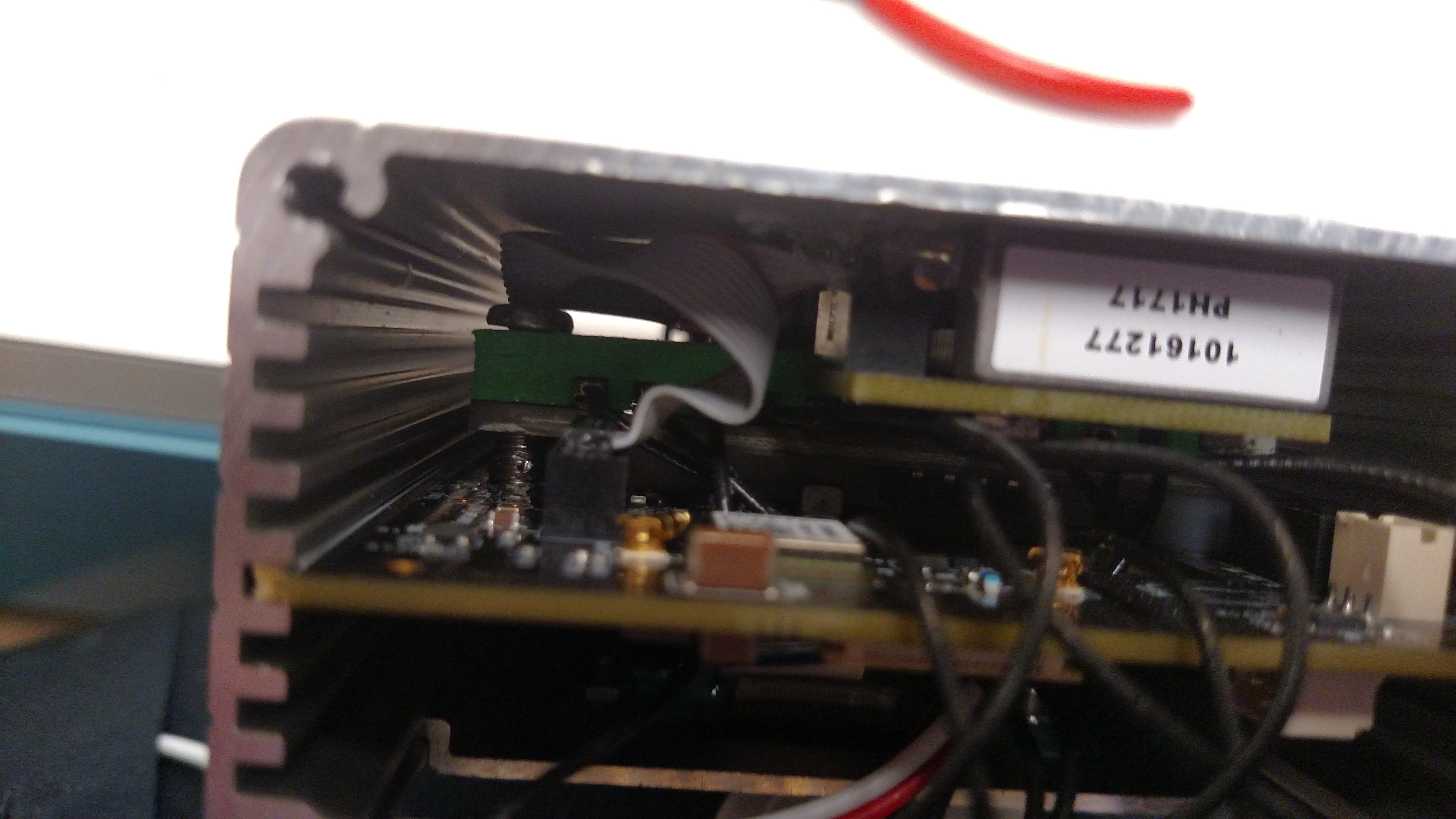
Apply hot glue to the cable and connector so it cannot be disconnected unintentionally. Let the glue dry for a minute.
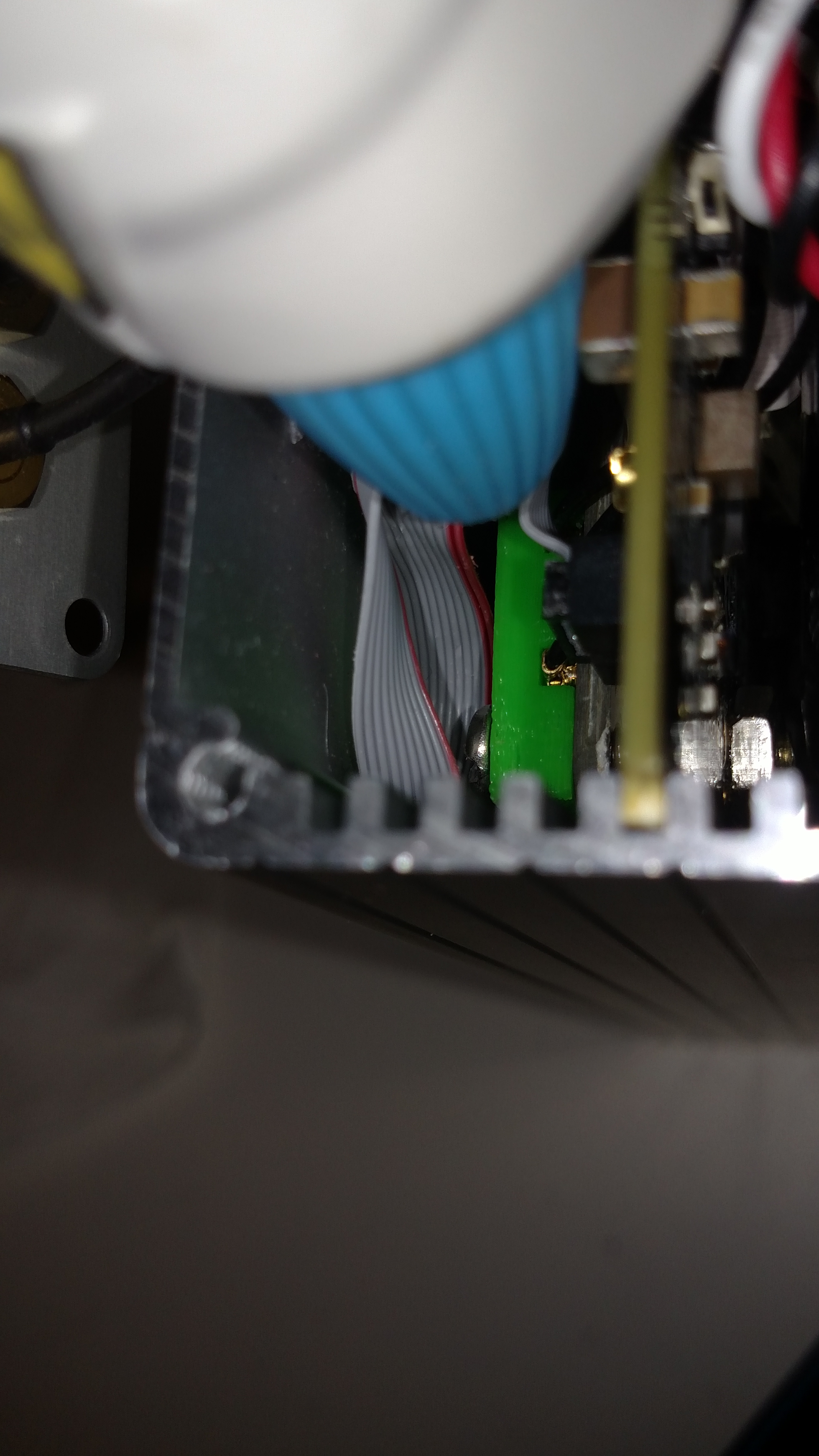
Face Plate
Make sure the button faces the same direction as the beveled screw holes on the face plate.
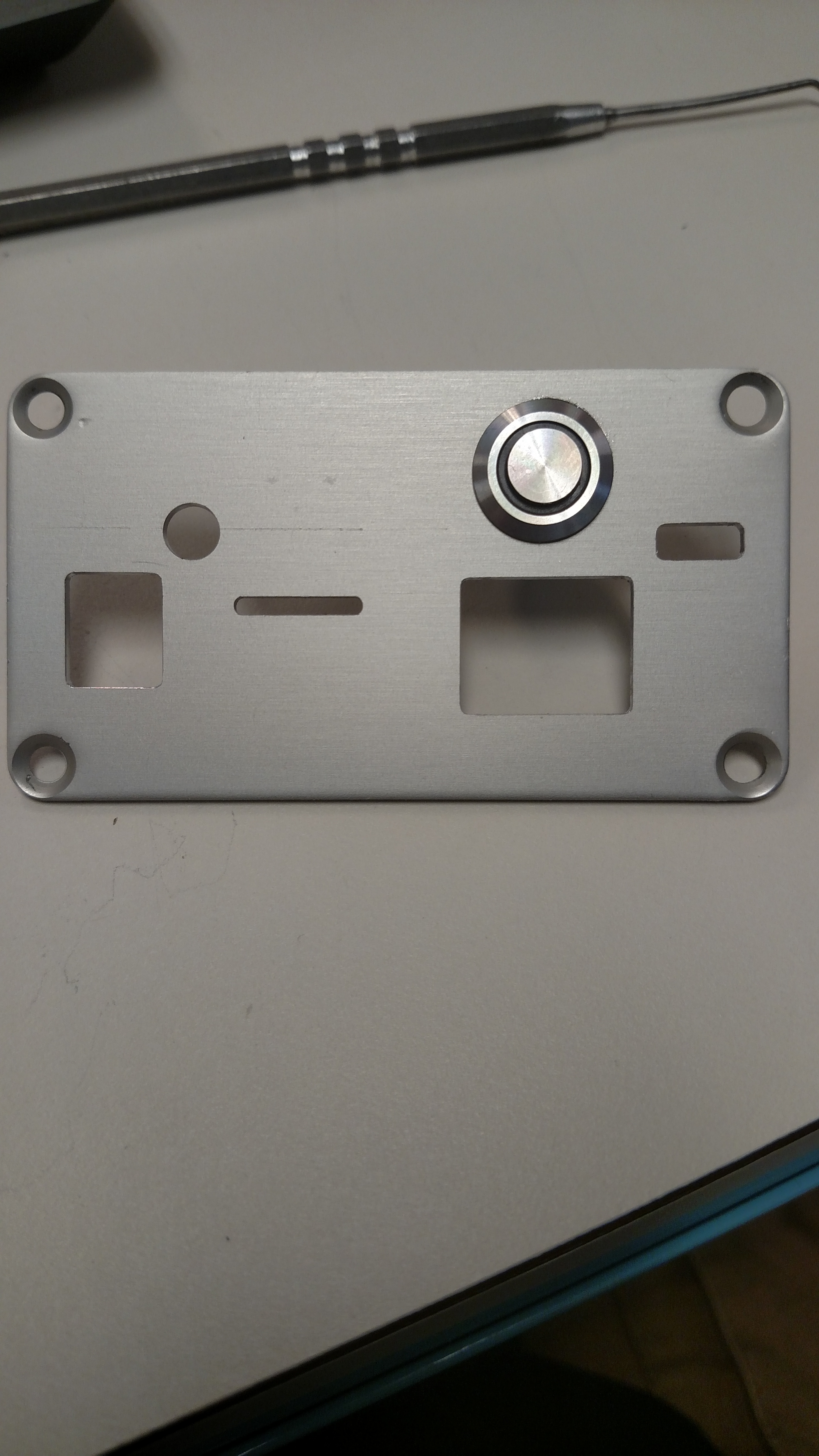
Add hex nut and tighten slightly.
Add the male pin header to the Power Switch Adapter PCB protruding TOWARD the face plate. Solder the pins.
Add the Power Switch Adapter PCB to the power switch. Solder the four pins.
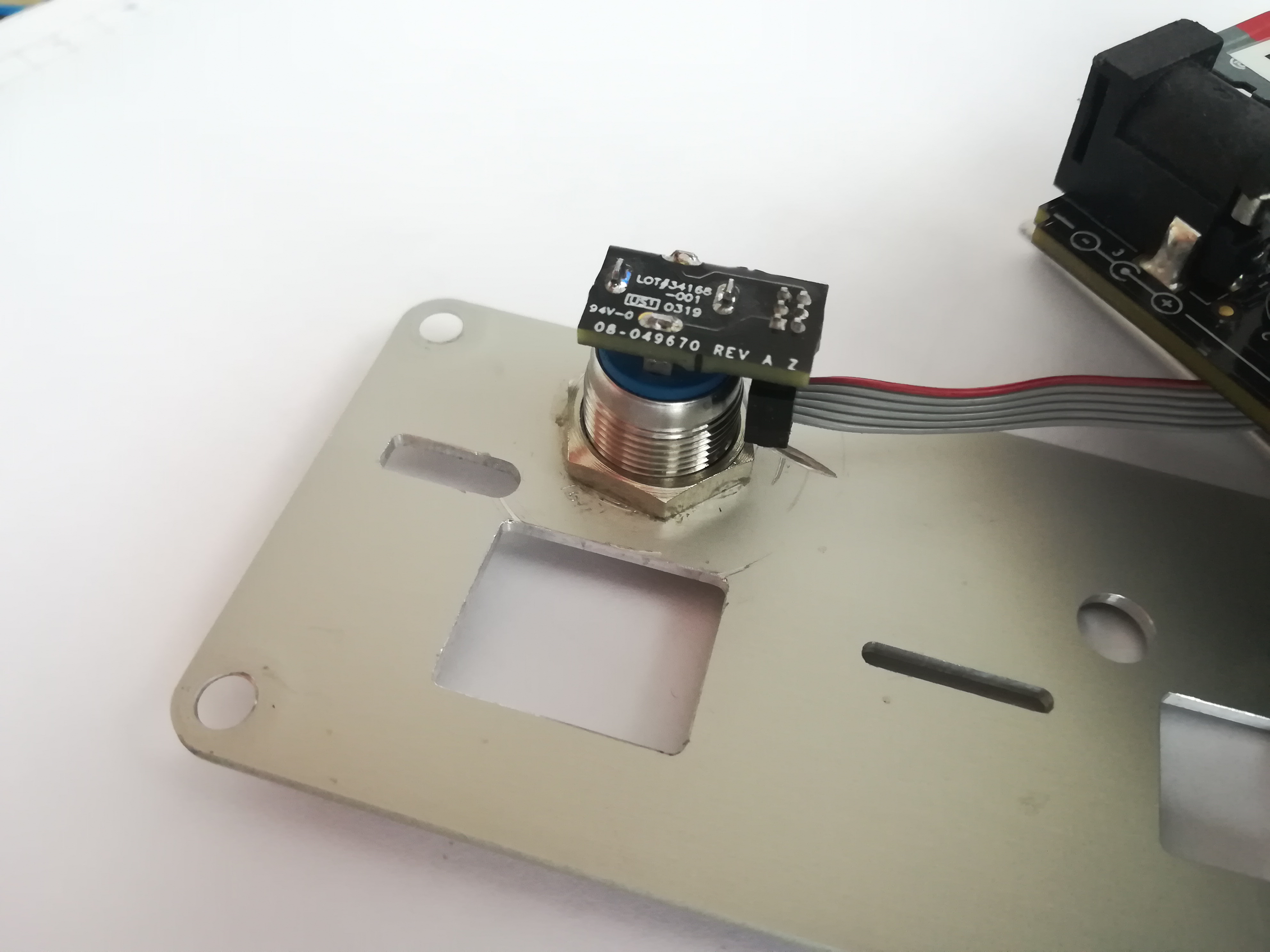
Attach the Power Switch Cable to the header.
Position the Power Switch Adapter PCB parallel to the bottom of the face plate. Position the hex nut parallel to the bottom of the face plate. Tighten the hex nut and apply Loctite.
Add hot glue to the connector on the Adapter PCB so the cable cannot be disconnected. Let the glue dry for a minute.
Connecting the Power Switch and Navigation Switch
Slide the belly plate away to access the Power Switch Connector (P9) and Navigation Switch Connector (P11).
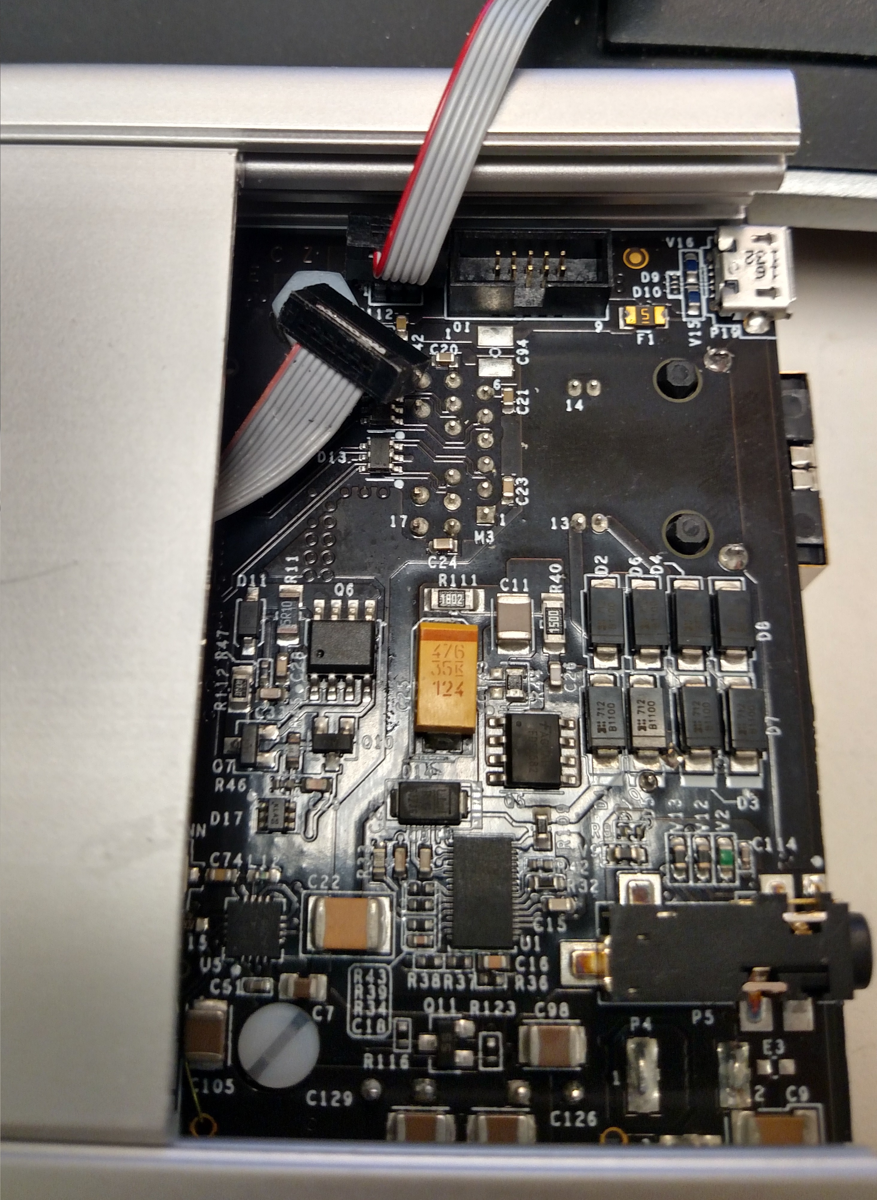
Connect the power switch cable to P9. Apply hot glue to the connector.
Note
Make sure no glue goes outside the white line in the silkscreen — this will make the PCB difficult to slide in and out.
Connect the navigation cable to P11.
Slide the case back to its starting position. Apply hot glue to the connector so it cannot be easily removed.
Adding the plastic frames
Position the plastic frame so one of the short sides of the face plate goes through the opening.
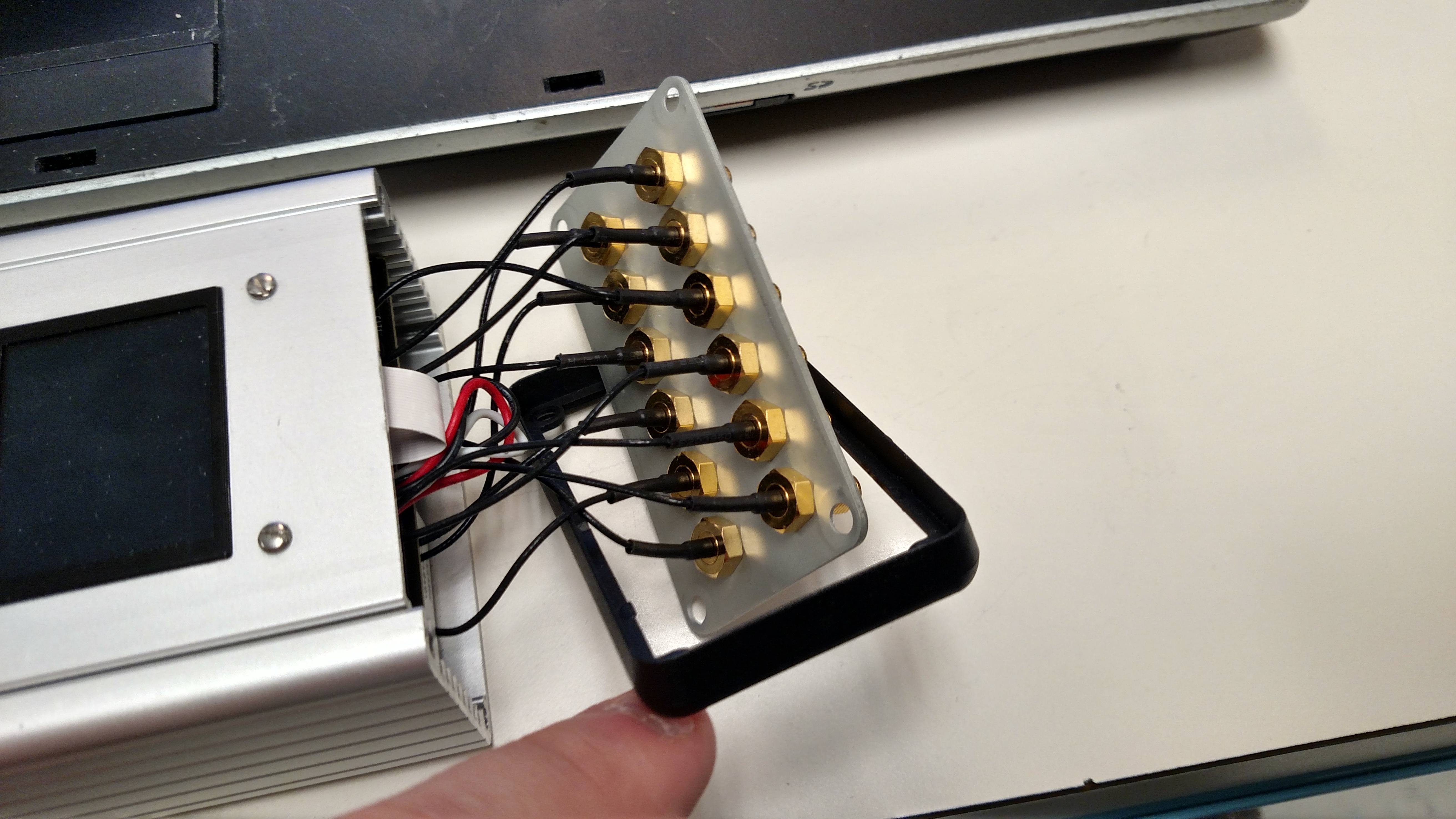
Gently push the face plate through the plastic frame.
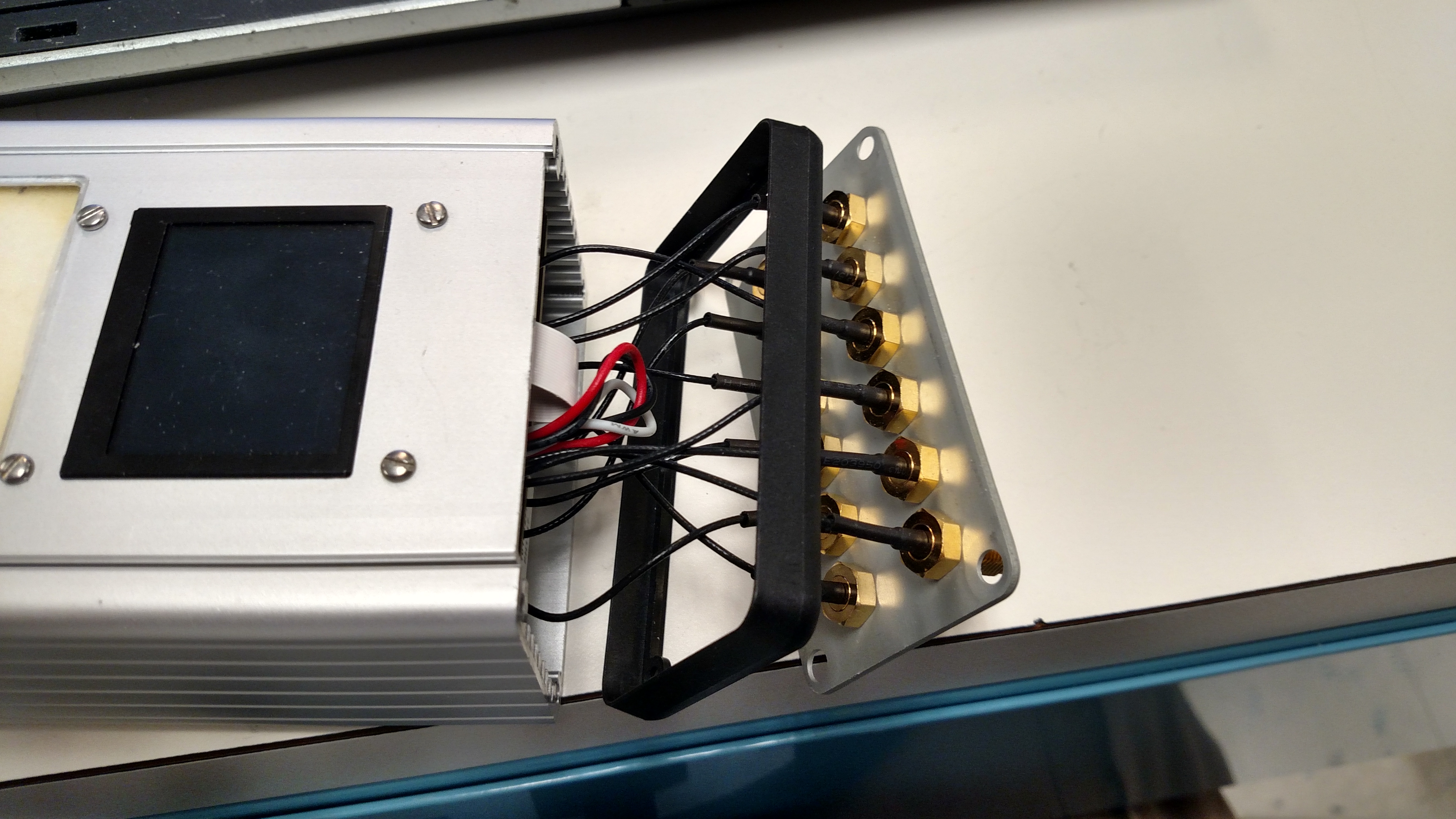
Push the plastic frame flush to the case.
Securing the face plates
SMA Face Plate
Ensure U.FL cables are not pinched or resting in any damaging condition. Make sure no U.FL cables are caught between the edge of the PCB and the face plate as you press it flush to the end of the case.
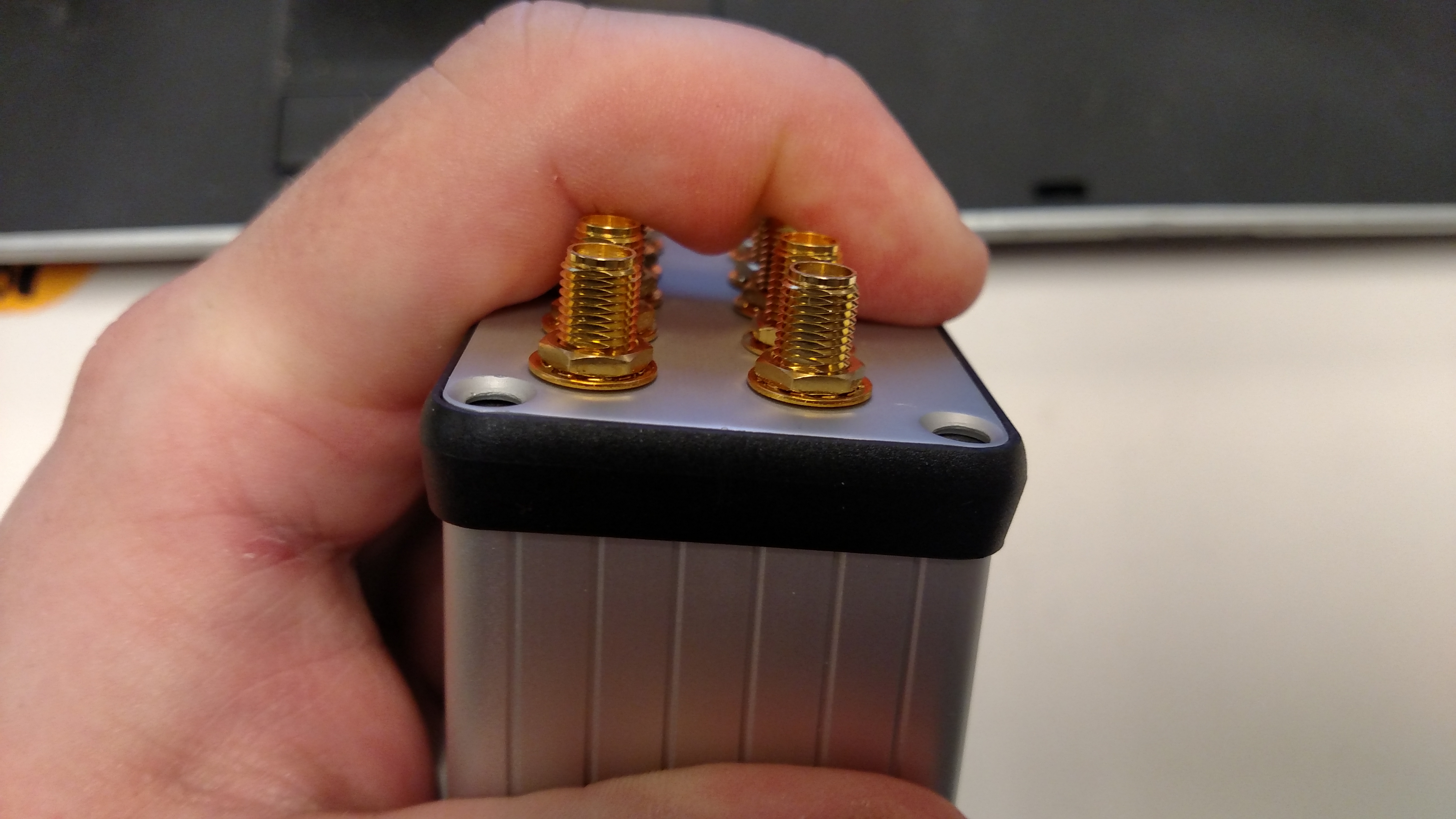
Insert screws and secure. Do not over-tighten — this risks stripping the threads.
Ethernet Face Plate
Make sure the connectors fit properly into the holes — they should be flush with no force required to align.
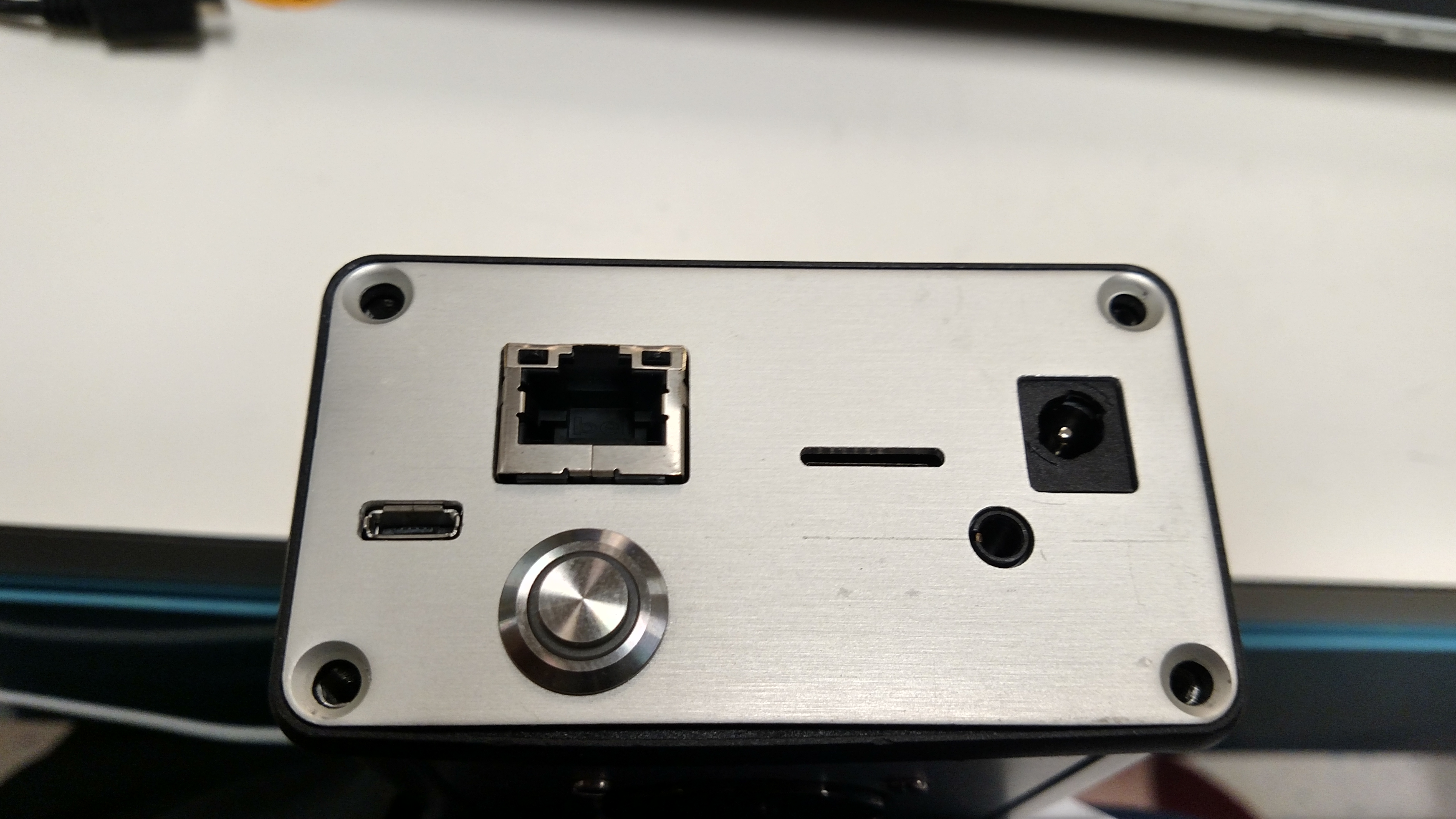
Insert screws and secure.
Adding Face Plate Labels
Two labels need to be added to the SMAs to match the text shown below (future builds will have silkscreen etched with the correct labels).
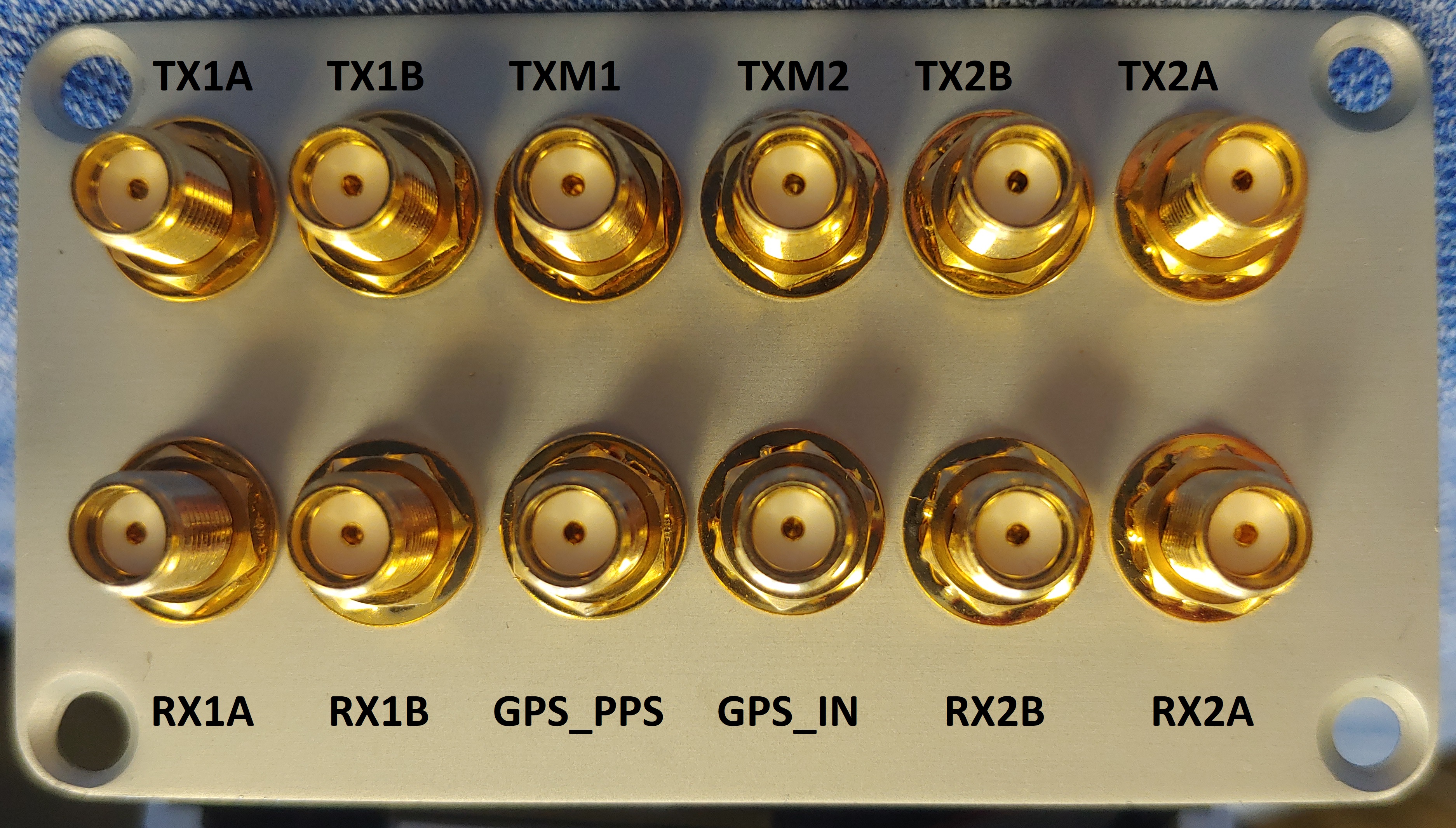
Once these steps are complete, begin the radio Full Assembly Test.
PackRF — Final Assembly
Place one finished radio in each slot (only one radio should have the JTAG adapter cable hanging out of the side).
Place one TPE-115GI POE injector in each slot.
Place 20 RF antennas in the slot.
Place the remaining items into the large open rectangle on the left (fold and press air out of plastic packaging so everything fits):
2× Micro SD cards
2× USB OTG cables
2× GPS antennas
2× Ethernet cables
2× Car adapters
2× DC wall warts
2× Webcams (de-boxed)
1× JTAG adapter
2× USB cables